Microstructure and method of manufacturing the same

a microstructure and microstructure technology, applied in the field of microstructure manufacturing, can solve the problems of insufficient raman signals, limited measurement size of substances, and difficult manufacturing of metallic nanostructural elements with pointed tips on a nanometer-order scale, and achieve the effect of enhancing electric field and enhancing electric field

Inactive Publication Date: 2009-04-16
FUJIFILM CORP
View PDF4 Cites 6 Cited by
  • Summary
  • Abstract
  • Description
  • Claims
  • Application Information

AI Technical Summary

Benefits of technology

[0030]According to a first embodiment of the second aspect of the invention, there can be provided a microstructure which is able to utilize the antenna effect to generate an enhanced electric field by having a metal microbody disposed on a base plate, the metal microbody including a columnar element which extends in a height direction and a divided projecting element which is provided at the tip portion continuous with the columnar element and has a multiply-divided branched shape that is narrower than the columnar element.
[0031]According to a second embodiment of the second aspect of the invention, there can be provided a microstructure which is able to utilize the antenna effect to generate an enhanced electric field by having a metal microbody disposed on a base plate, the metal microbody having an outside diameter that narrows from a base end on the base plate side toward a tip portion having a projection with a sharply tapered shape.
[0032]Since an enhanced electric field is generated by the antenna effect in a region peripheral to a narrower projection, such as a pointed tip, the microstructures according to the first and second embodiments of the second aspect of the invention are not subject to size limitations for the substance placed in the enhanced electric field generating region. Even large-size substances, such as those exceeding 10 nm that have been difficult to place inside the enhanced electric field generating region in a microstructure which utilizes the proximity effect, can be easily placed within the enhanced electric field generating region.

Problems solved by technology

If the size of the substance to be measured is larger than the interstices, the substance to be measured does not enter the interstices, as a result of which a SERS effect cannot be suitably achieved, making it impossible to obtain sufficient Raman signals.
That is, when the proximity effect is employed, there are limitations on the size of the substance to be measured.
Yet, manufacturing metallic nanostructural elements that have pointed tips on a nanometer-order scale is very difficult.
However, even when a metal is coated onto the surface of the zinc oxide needles, obtaining a uniform metal coat at the tips of the needles is not easy, making it a considerable challenge to manufacture metallic nanostructural elements having pointed tips.

Method used


Image

  • Microstructure and method of manufacturing the same
  • Microstructure and method of manufacturing the same
  • Microstructure and method of manufacturing the same

Examples


examples

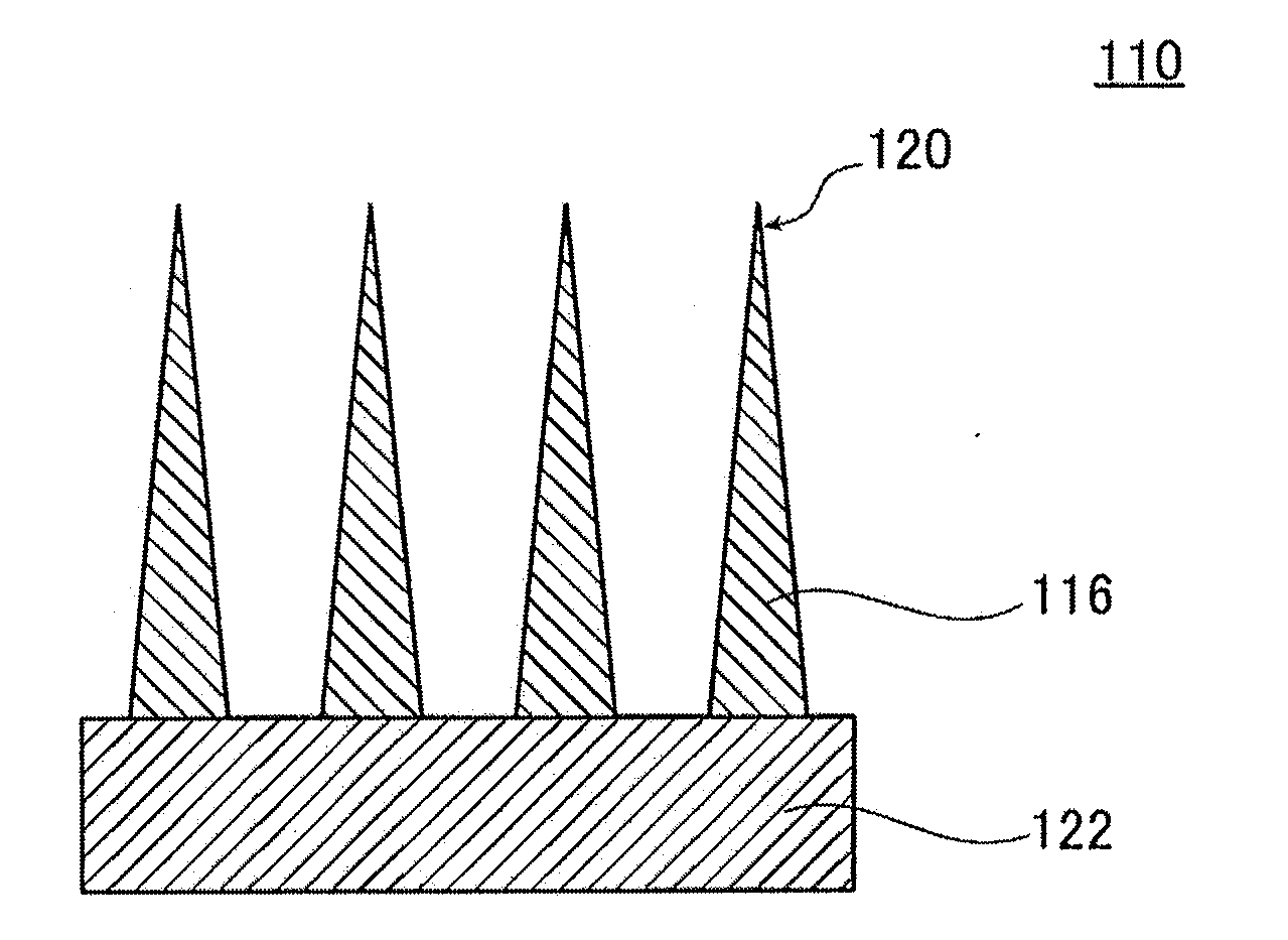
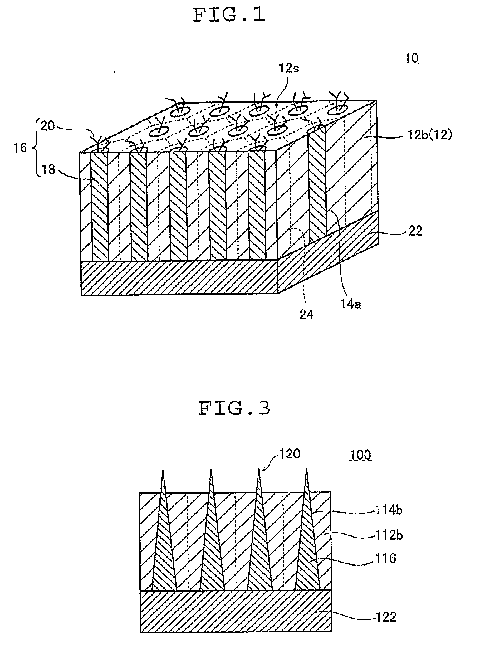
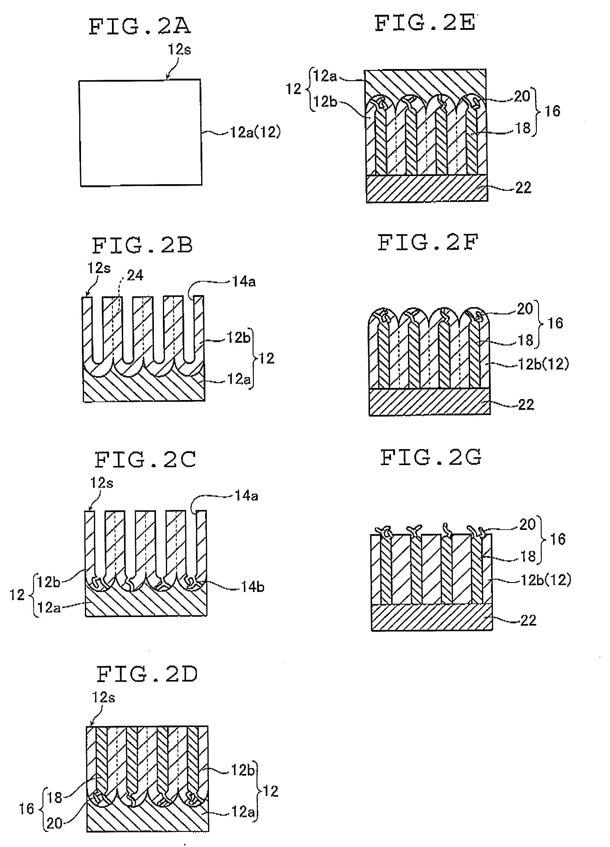
[0122]The microstructure 10 shown in FIG. 1 was manufactured by the microstructure manufacturing method shown in FIG. 2.

[0123]In this example, aluminum (Al) was used as the anodizable metal substrate. Anodizing treatment was carried out on this anodizable aluminum substrate. In the present example, the anodizing treatment conditions were as follows: oxalic acid as the electrolytic solution, an electrolytic solution concentration of 0.5 M, a solution temperature of 15° C., and an applied voltage of 40 V.

[0124]Next, current recovery treatment was carried out under the following conditions: steps in which the voltage was lowered by 5 volts per step were carried out from 35 V down to 15 V. In this current recovery treatment, the results of current value measurements, which indicate the state of current value recovery, are shown in the graph in FIG. 6.

[0125]Next, electroplating treatment was carried out, thereby filling gold (Au) into the micropores and forming metal microbodies. Electro...


PUM

PropertyMeasurementUnit
sizeaaaaaaaaaa
diameteraaaaaaaaaa
diameteraaaaaaaaaa

Abstract

The method of manufacturing a microstructure having metal microbodies which generate an enhanced electric field includes forming, in a substrate, micropores each of which opens out on a surface of the substrate, has an inside diameter that varies in a depth direction, and has in a tip portion thereof a narrower, outwardly projecting recess, filling the micropores with metal to form the metal microbodies each having at a tip portion thereof a projection made of the metal filled into the outwardly projecting recess, and removing at least part of the substrate from a metal microbody tip portion side to expose at least the projection at the tip portion of each of the metal microbodies. The resulting microstructure has metallic nanostructural elements that generate an enhanced electric field by an antenna effect at their pointed tips.

Description

[0001]The entire contents of all documents cited in this specification are incorporated herein by reference.BACKGROUND OF THE INVENTION[0002]The present invention relates to a method of manufacturing a microstructure having metal microbodies which generate an enhanced electric field, and to a microstructure manufactured by such a method.[0003]Raman spectroscopy is a technique, used for identifying substances and other purposes, in which scattered light obtained by irradiating a substance with monochromatic light is spectrally analyzed to give a spectrum of Raman scattered light (a Raman spectrum). Because such Raman scattered light is very weak, a method for achieving a surface-enhanced Raman scattering (SERS) effect has been proposed, wherein such Raman scattered light is enhanced by utilizing the local plasmon resonance (plasmon effect) that arises from nanometer-order metallic microstructural elements (referred to below as a “metallic nanostructural elements”).[0004]In addition, ...

Claims


Application Information

Patent Timeline
Patent Type & Authority Applications(United States)
IPC IPC(8): B32B3/00B44C1/22
CPCY10T428/24612G01N21/658
Inventor TOMARU, YUICHI
Owner FUJIFILM CORP
Why Eureka
Try Eureka