Chip bonding pad of integrated circuit, manufacture method thereof and integrated circuit comprising bonding pad

A technology of an integrated circuit and a manufacturing method, which is applied in the field of anti-antenna effect chip pad structure and its manufacturing, and can solve problems such as affecting circuit performance and inappropriateness.

Active Publication Date: 2009-12-30
TSMC CHINA COMPANY
View PDF0 Cites 5 Cited by
  • Summary
  • Abstract
  • Description
  • Claims
  • Application Information

AI Technical Summary

Problems solved by technology

[0007] However, the above-mentioned method of utilizing the interconnection metal layer, diode breakdown and metal jumper is not very effective in avoiding the antenna effect of the integrated circuit chip bonding pad, at least including the following reasons. First, the method of utilizing diode breakdown may require Changing the circuit design of the original integrated circuit affects the performance of the circuit, which will be described in more detail in the following content. Second, the bonding surface of the chip pad is usually formed on the uppermost conductive pad layer, and the metal straddle is formed on it. The wiring is not suitable

Method used


Image

  • Chip bonding pad of integrated circuit, manufacture method thereof and integrated circuit comprising bonding pad
  • Chip bonding pad of integrated circuit, manufacture method thereof and integrated circuit comprising bonding pad
  • Chip bonding pad of integrated circuit, manufacture method thereof and integrated circuit comprising bonding pad

Examples


Embodiment Construction

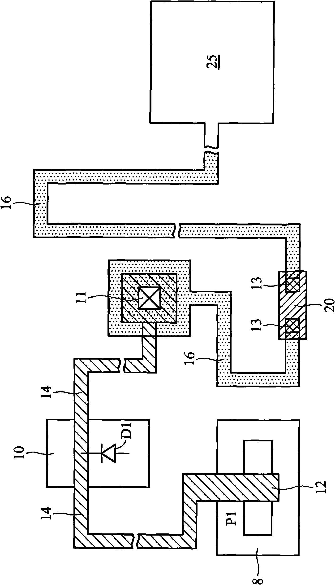
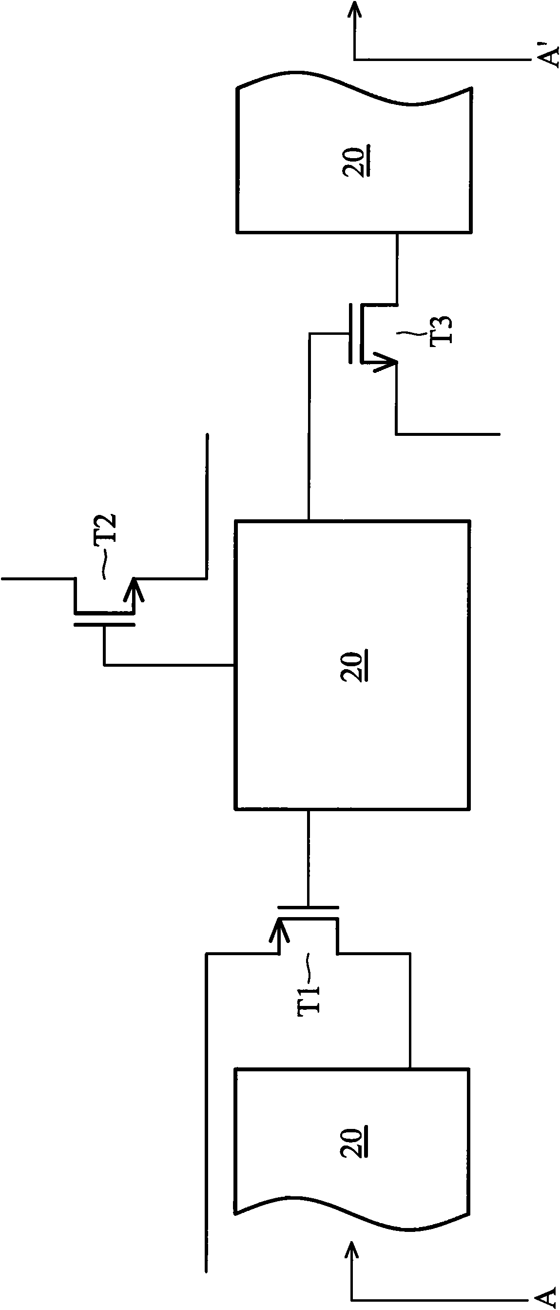
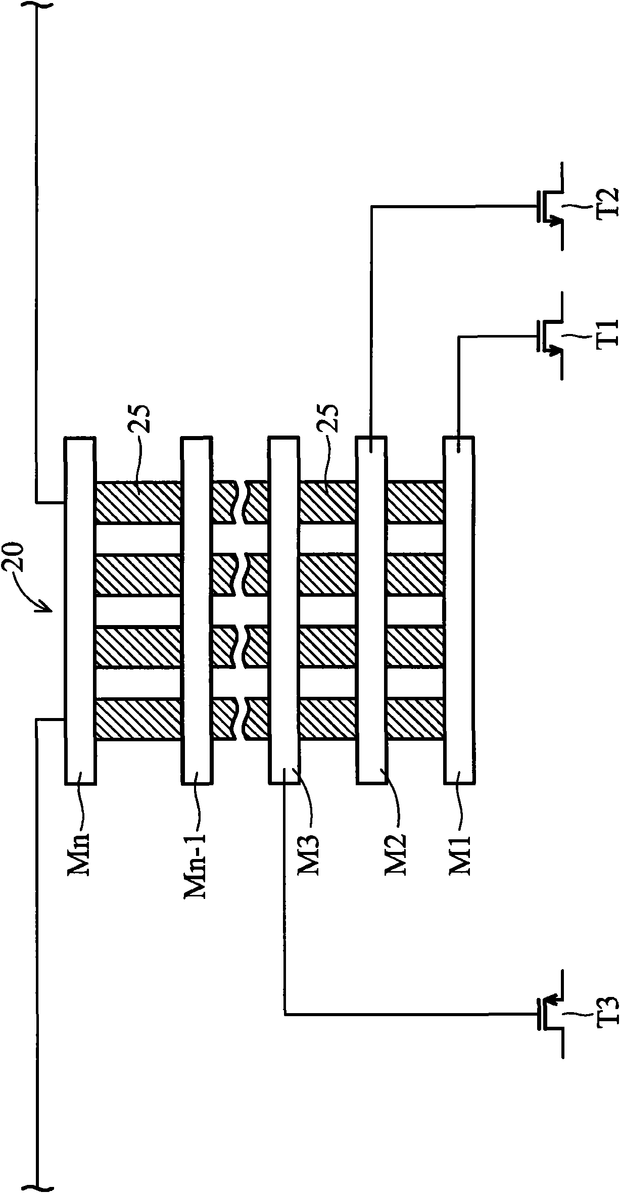
[0100] Preferred embodiments of the related content of the present invention will be described below, mainly the chip pad structure and the method of resisting the antenna effect. The preferred embodiment includes probe pads on a parametric test line, typically formed on a wafer in the area between adjacent integrated circuit dies, for measuring electrical characteristics of components formed on the integrated circuit. Preferred embodiments also include bonding pads on an integrated circuit bonded to metal wires and electrically connected to an integrated circuit package. The anti-antenna effect chip pad structure in the preferred embodiment does not include other manufacturing process steps outside the integrated circuit manufacturing flow.

[0101] Figure 2A It is a partial top view of a semiconductor integrated circuit chip, on which a plurality of chip bonding pads 20 are formed. The chip pad 20 includes a large surface layer, usually formed on the uppermost conductive ...


PUM


Abstract

The invention provides an integrated circuit, a chip bonding pad structure and a manufacture method. The chip bonding pad comprises a main bonding pad and a ring bonding pad. In a process of fabricating charges comprising formation of the chip bonding pad, a grid of a metal oxide semiconductor transistor in a substrate of the integrated circuit is electrically connected with the ring bonding pad,therefore area ratio from an antenna to the grid is less than a proportion of a given antenna, thus effectively reducing or avoiding antenna effect. The main bonding pad is electrically coupled with the ring bonding pad through a metal bridge formed in an upper inside cable metal layer or an uppermost conductive bonding pad layer. The chip bonding pad provided by the invention is a probe bonding pad on a parameter testing line or a bonding pad on the integrated circuit.

Description

technical field [0001] The invention relates to a manufacturing method of an integrated circuit, in particular to an anti-antenna effect chip bonding pad structure arranged in an integrated circuit and a manufacturing method thereof. Background technique [0002] In the manufacturing process of using metal oxide semiconductor technology to manufacture integrated circuits, it usually includes a manufacturing process using charged ions, such as a plasma etching manufacturing process or an ion implantation manufacturing process, for example, in a gate polysilicon pattern or In the plasma etching manufacturing process of the interconnect metal wiring pattern, static charges will accumulate on a floating gate polysilicon electrode, which will greatly increase the voltage intensity of the gate polysilicon electrode, causing the charge to flow into the gate oxide layer and trap it in the gate oxide layer or across the gate oxide layer. The above-mentioned charges will greatly redu...

Claims


Application Information

Patent Timeline
Patent Type & Authority Applications(China)
IPC IPC(8): H01L23/485H01L23/488H01L23/58H01L21/60H01L21/768
CPCH01L24/05H01L2224/02166H01L2224/05093H01L2224/05552H01L2224/05554H01L2924/13091H01L2924/14
Inventor 翁武得聂吉祥
Owner TSMC CHINA COMPANY
Why Eureka
Try Eureka