
Coreless packaging substrate, pop structure, and methods for fabricating the same

a packaging substrate and coreless technology, applied in the direction of semiconductor devices, semiconductor/solid-state device details, electrical equipment, etc., can solve the problems of high fabrication cost, short circuit, and inability to meet the thinning requirement, so as to reduce the use of solder materials, reduce material and fabrication costs, and prevent bridging

Inactive Publication Date: 2015-11-12
SILICONWARE PRECISION IND CO LTD
View PDF4 Cites 12 Cited by
  • Summary
  • Abstract
  • Description
  • Claims
  • Application Information

AI Technical Summary

Benefits of technology

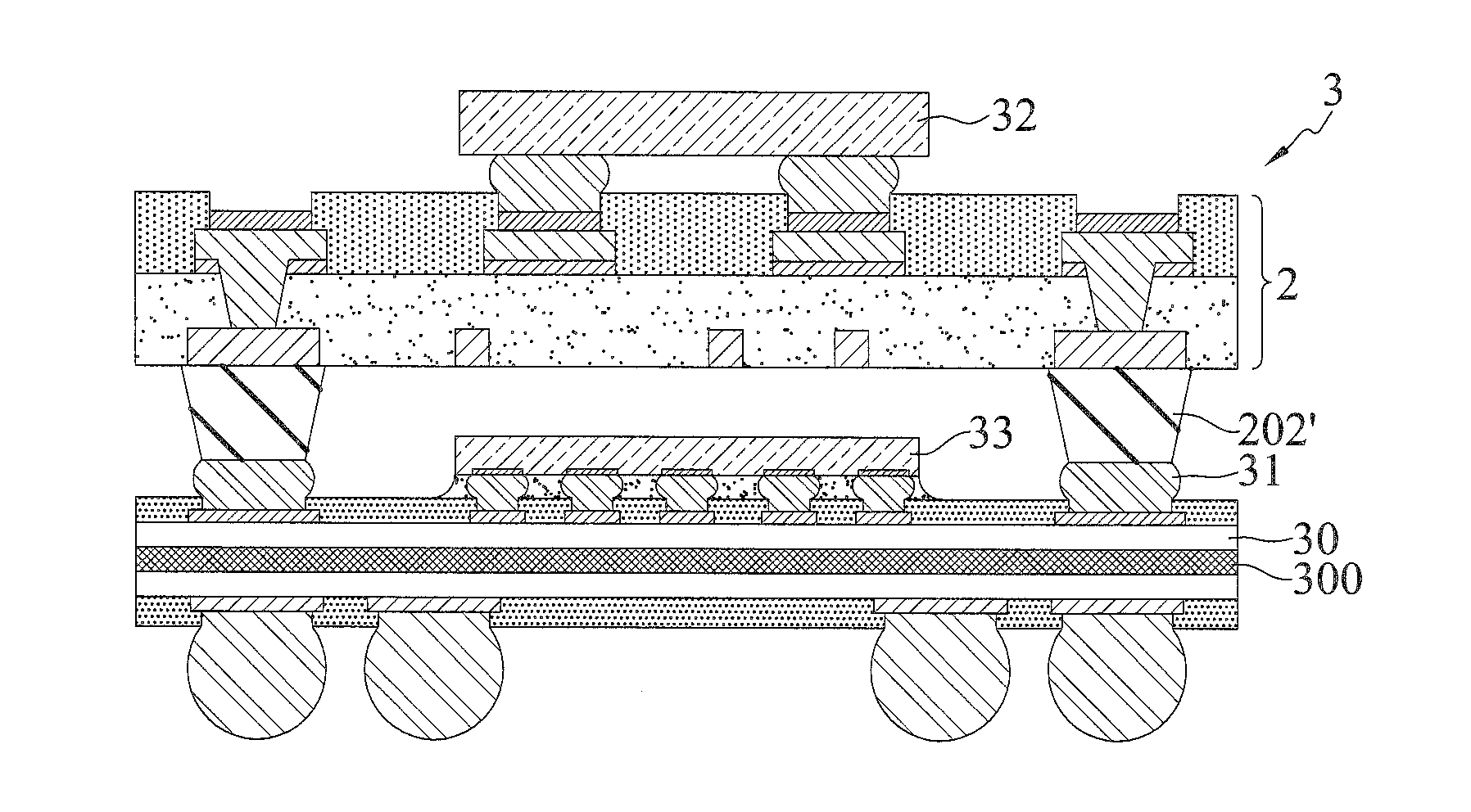
The present invention provides a method for making a circuit structure without a core layer, reducing material and fabrication costs. By using conductive elements and stacking the board and packaging substrate, bridging is prevented, allowing for smaller connections and increasing product yield. This method also reduces the use of solder material, meeting the fine pitch requirement.

Problems solved by technology

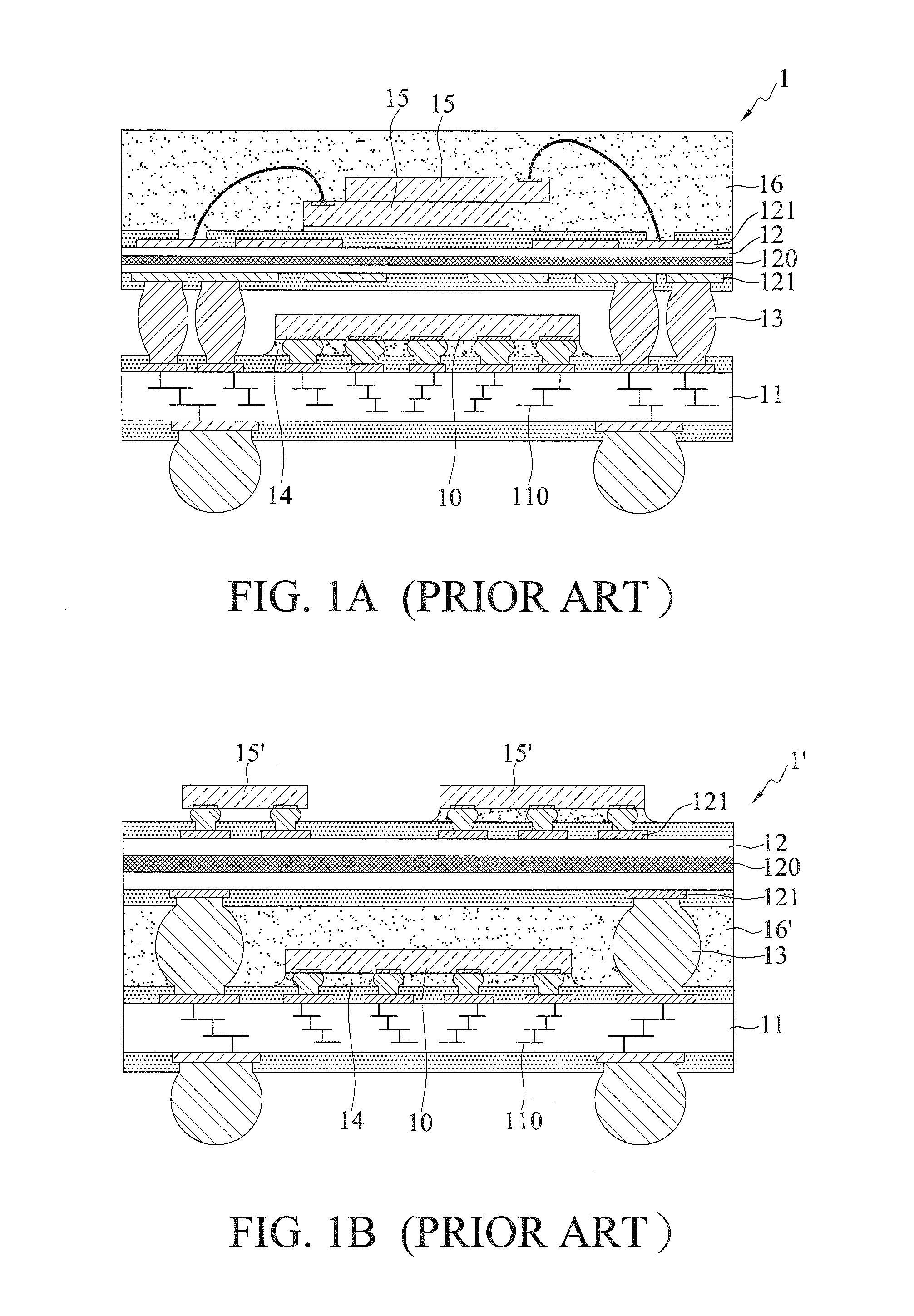
However, in the PoP structures 1, 1′, the second packaging substrate 12 having a core layer incurs a high fabrication cost and cannot meet the thinning requirement.
As such, solder bridging easily occurs between the solder balls 13, thus incurring a short circuit and reducing the product yield and reliability.
That is, size variation of the solder balls 13 is not easy to control.
As such, defects may occur to solder joints and result in a poor electrical connection quality.
Therefore, solder bridging easily occurs between adjacent solder balls 13, thereby reducing the electrical connection quality.
In addition, the solder balls 13 arranged in a grid array may have a poor coplanarity.

Method used


Image

  • Coreless packaging substrate, pop structure, and methods for fabricating the same
  • Coreless packaging substrate, pop structure, and methods for fabricating the same
  • Coreless packaging substrate, pop structure, and methods for fabricating the same

Examples


Embodiment Construction

[0029]The following illustrative embodiments are provided to illustrate the disclosure of the present invention, these and other advantages and effects can be apparent to those in the art after reading this specification.

[0030]It should be noted that all the drawings are not intended to limit the present invention. Various modifications and variations can be made without departing from the spirit of the present invention. Further, terms such as “first”, “second”, “on”, “a” etc. are merely for illustrative purposes and should not be construed to limit the scope of the present invention.

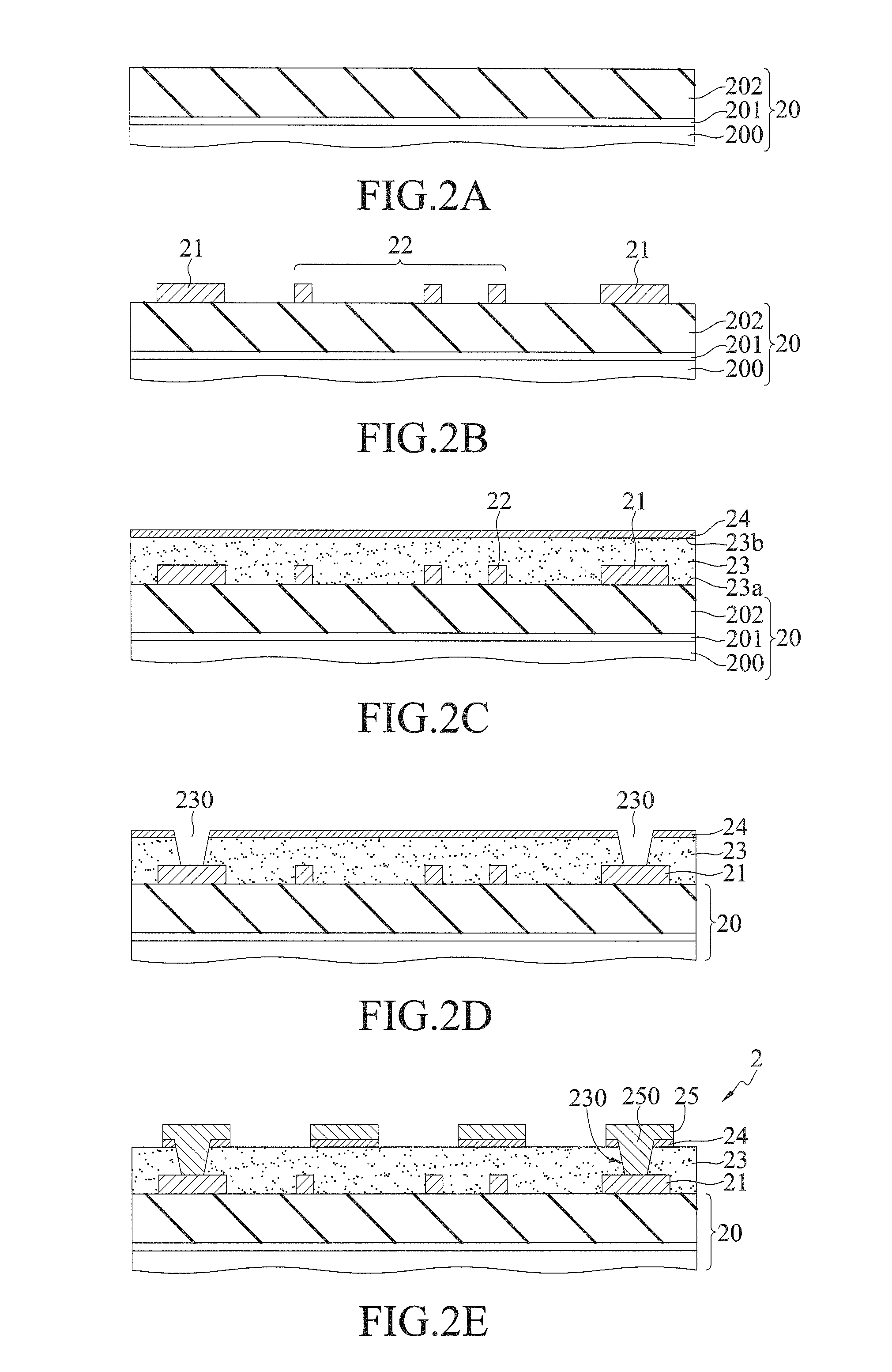
[0031]FIGS. 2A to 2H are schematic cross-sectional views showing a method for fabricating a coreless packaging substrate 2 according to a first embodiment of the present invention.

[0032]Referring to FIG. 2A, a carrier 20 is provided. The carrier 20 has a substrate 200, a release layer 201 formed on the substrate 200, and a conductive plate 202 disposed on the release layer 201.

[0033]In an embodiment, t...


PUM


Abstract

A method for fabricating a coreless packaging substrate is provided, which includes: forming a dielectric layer on a conductive plate having a plurality of conductive pads; forming a circuit layer on the dielectric layer and forming in the dielectric layer a plurality of conductive vias that electrically connect the circuit layer and the conductive pads; and removing a portion of the conductive plate so as to cause the remaining portion of the conductive plate to form a plurality of conductive elements, thereby dispensing with a core layer and reducing the material and fabrication cost.

Description

BACKGROUND OF THE INVENTION[0001]1. Field of the Invention[0002]The present invention relates to PoP (package on package) structures, and, more particularly, to a PoP structure with improved product yield and a method for fabricating the same.[0003]2. Description of Related Art[0004]Along with the progress of semiconductor packaging technologies, various package types have been developed for semiconductor devices. To improve electrical performances and save spaces, a plurality of packages can be stacked to form a package on package (PoP) structure. Such a packaging method allows merging of heterogeneous technologies in a system-in-package (SiP) so as to systematically integrate a plurality of electronic components having different functions, such as a memory, a CPU (Central Processing Unit), a GPU (Graphics Processing Unit), an image application processor and so on, and therefore is applicable to various thin type electronic products.[0005]FIGS. 1A and 1B are schematic cross-section...

Claims


Application Information

Patent Timeline
IPC IPC(8): H01L23/522H01L21/56H01L23/482H01L23/31H01L23/498H01L21/768
CPCH01L23/5226H01L23/49822H01L21/56H01L23/4824H01L23/3157H01L21/76897H01L23/49811H01L23/49833H01L21/48H01L23/5389H01L2924/181H01L2224/32225H01L2224/48091H01L2224/48227H01L2224/73204H01L2924/15311H01L23/3128H01L25/105H01L25/50H01L2224/16237H01L2924/00014H01L2924/00012H01L2224/16225H01L2924/00
Inventor LIN, CHUN- HSIENCHIU, SHIH-CHAOPAI, YU-CHENGSHEN, TZU-CHIEHSUN, MING-CHEN
Owner SILICONWARE PRECISION IND CO LTD
Learn More