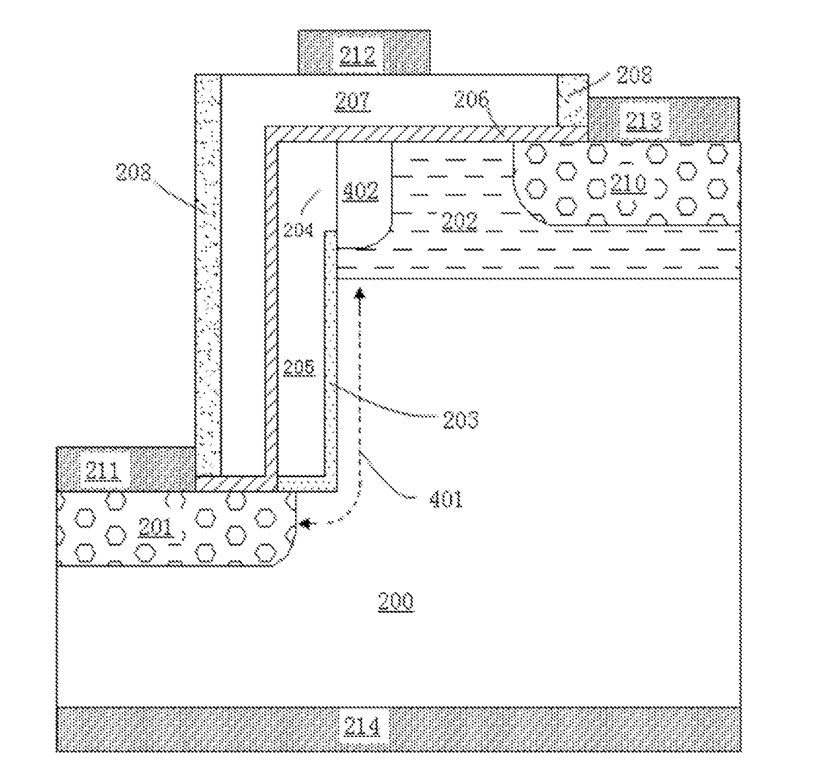
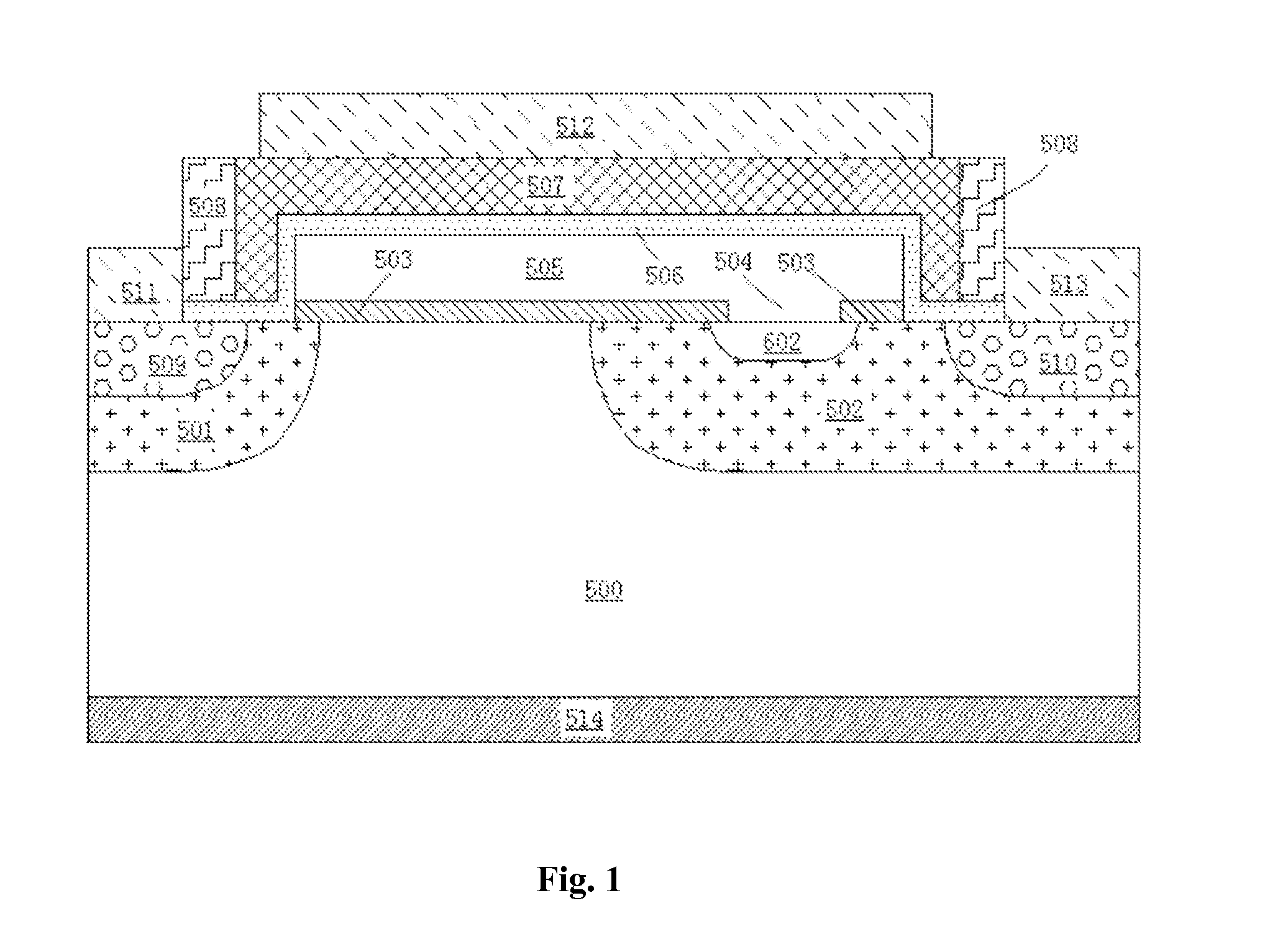
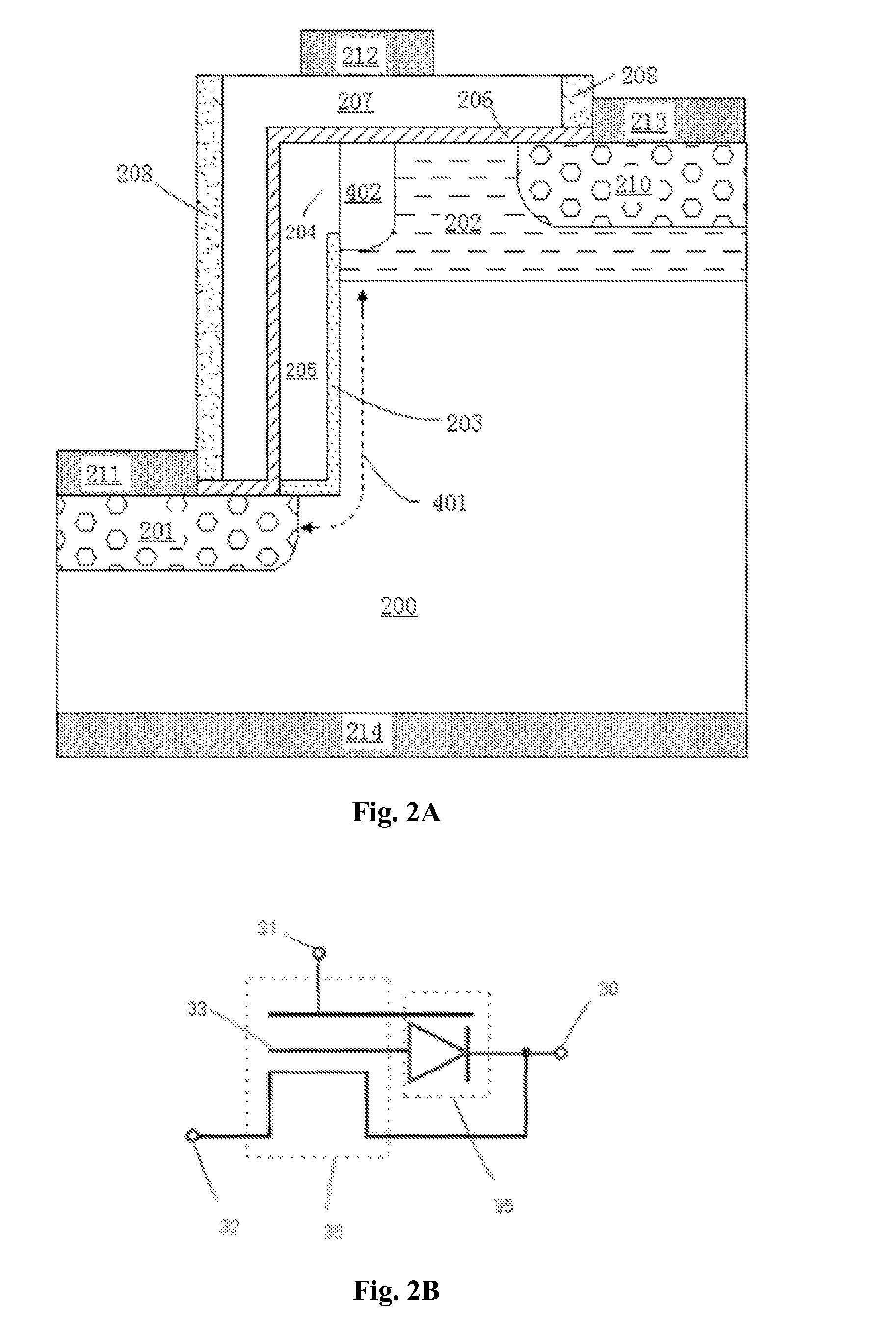
[0038]The disclosure is further detailed in combination with the drawings and the embodiments. In the figures, to facilitate illustration, the thickness of the layer and region is magnified, so the size does not represent the actual dimension. The reference figures are the schematic views of a typical embodiment for the disclosure. The embodiment shall not be limited to the specific sizes in the regions shown in the figures, but include all the shapes obtained, for example, a size with a deviation caused in manufacturing. For instance, the curve obtained through etching is generally bent or round. However, in the embodiment of the disclosure, it is indicated by a rectangle, which shall not be regarded as a limit to the scope of the disclosure.
[0039]FIG. 2a show three sectional views of an embodiment of the semi-floating-gate device disclosed in the disclosure along the length direction the device's channel. As shown in FIG. 2a, the semi-floating-gate device disclosed in the disclosure comprise a semiconductor substrate 200 with the first doping type and a perpendicular channel region 401 formed in the semiconductor substrate, wherein the perpendicular channel region 401 is an inversion layer formed in the semiconductor substrate 200 when the semiconductor device works. A source region 201 with the second doping type is formed in the bottom of the perpendicular channel region 401 and a drain region 202 with the second doping type is formed in the top of the perpendicular channel region 401. The semiconductor substrate 200 can be made of monocrystalline silicon, polysilicon or silicon on insulator. The first doping type is n type, the second doping type is p type, alternatively, the first doping type is p type, and the second doping type is n type.
[0040]A first layer of insulation film 203 formed due to covering the source region, the drain region and the perpendicular channel region. A floating gate opening region 204 formed due to covering the first layer of insulation film 203 of the drain region 202 in the top of the perpendicular channel region 401. The first layer of insulation film 203 may be made of silicon dioxide, silicon nitride, silicon oxynitride, or insulation materials with high dielectric constant, and the physical thickness preferably ranges from 1 nm to 20 nm.
[0041]A floating gate 205 with the first doping type used as a charge storage node is above the first layer of insulation film 203 formed due to covering the channel region 401 and the floating gate opening region 204. The floating gate 205 has the doping type opposite to that of the drain region 202. The doped impurities in the floating gate 205 can be diffused into the drain region 202 through the floating gate opening region 204 to further form a diffusion region 402 with the first doping type, thus a p-n junction diode is formed between the floating gate 205 and the drain region 202 through the floating gate opening region 204.
[0042]A second layer of insulation film 206 is formed due to covering the floating gate 205 and the p-n junction diode structure, wherein the second layer of insulation film 206 may be made of silicon dioxide, silicon nitride, silicon oxynitride or insulation materials with high dielectric constant, and the physical thickness preferably ranges from 1 nm to 20 nm.
[0043]A control gate 207 which lies above the second layer of insulation film 206 is formed due to covering the floating gate 205 and the p-n junction diode, wherein the control gate 207 can be made of metal, alloy or doped polysilicon.
[0044]Number 208 is a side wall of the gate of the device made of silicon dioxide or silicon nitride. The side wall 208 is a well-known structure in this field for isolating the control gate 207 from other conducting layers of the device.
[0045]A doping region 210 is formed in the drain region 202, wherein the doping type of the doping region 210 is same to that of the drain region 202. The doping regions 210 have a doping concentration greatly higher than that of the source region 202 so as to reduce the ohmic contact of device.
[0046]The semi-floating-gate device disclosed in the disclosure further comprises the contactor of the source region 211, the contactor of the control gate 212, the contactor of the drain region 213 and the contactor of the semiconductor substrate 214 made of conducting materials are used to connect the source region 201, the control gate 207, the drain region 202 and the semiconductor substrate 200 with the external electrode.
[0047]In order to further detail the structure and function of the semi-floating-gate device disclosed in the disclosure, FIG. 2b shows an equivalent circuit diagram of the semi-floating-gate device. As shown in FIG. 2b, the semi-floating-gate device disclosed in the disclosure comprises a MOSFET 36 and a gated diode 35 with the control gate 31 of MOSFET 36 as the gate, wherein the MOSFET 36 has source electrode 32, drain electrode 30, floating gate 33 and control gate 31. The floating gate 33 of MOSFET 36 can be connected with the anode or cathode of the gated diode 35. In the embodiment of the disclosure shown in the FIG. 2b, the floating gate 33 is connected with the anode of the gated diode 35. The floating gate 33 is charged or discharged by the gated diode 35 to change the number of the charges in the floating gate 33. The number of the charges determines the logic state of the semi-floating-gate device, and that means it has current or not in the perpendicular channel region.
[0048]The semi-floating-gate device disclosed in the disclosure can be manufactured via many methods. The description below is the flow chart for manufacturing an embodiment of the semi-floating-gate device with n-type channel shown in FIG. 2a.
[0049]Firstly, as shown in FIG. 3, form a source region (not shown) in the semiconductor substrate 200 with the first doping type through the shallow trench isolation (STI) process. This STI process is well known in this field. Conduct ion injection of the second doping type into the semiconductor substrate 200 to form a lightly-doped region 300. The semiconductor substrate 200 can be made of monocrystalline silicon, polysilicon or silicon on insulator. The first doping type is p type, and the second doping type is n type.
[0050]Afterwards, deposit a hard mark layer 301 on the surface of the semiconductor substrate, wherein the hard mark layer 301 can be made of silicon nitride. Then deposit a layer of optical resist 302 on the hard mark layer 301, and expose and develop it to define the position of the perpendicular channel region for device, and etch out the exposure hard make layer 301, and etch out the exposure semiconductor substrate 200 by using the hard mask layer as mask to form the perpendicular channel region in the semiconductor substrate 200. The etching depth is greater than the depth of the lightly-doped region 300 with the second doping type. After etching, one part of the lightly-doped region 300 with the second doping type will be left to form a drain region 202 for the device, shown as FIG. 4.
[0051]Afterwards, remove the optical resist 303 and continue to etch out the left hard mask layer 301, and then form a first layer of insulation film 203 on the surface of the exposure semiconductor substrate 200, wherein the first layer of insulation film 203 can be made of silicon dioxide, silicon nitride, silicon oxynitride or insulation materials with high dielectric constant, and the physical thickness preferably ranges from 1 nm to 20 nm. Then, deposit a layer of optical resist on the insulation film 203, and define the location of the floating gate opening region via the photolithographic process, and etch out the first layer of insulation film 203 exposed to form the floating gate opening region 204. FIG. 5 shows the condition after the optical resist is removed.
[0052]Next, deposit and form a first layer of conducting film on the exposure surface of the structure formed, wherein the conducting film is made of polysilicon with p-type doping type. Then, form a floating gate 205 via etching the first layer of conducting film, wherein the floating gate 205 at least covers the perpendicular channel region and the floating gate opening region 204. The impurities doped in the floating gate 205 may be diffused into the drain region 202 through the floating gate opening region 204 below the floating gate 205 to form p-type diffusion region 402, and a p-n junction diode is formed between the floating region 205 and the drain region 202 through the floating gate opening region 204. FIG. 6 shows the condition after the optical resist is removed.
[0053]Next, continue to etch out the first layer of insulation film 203 exposed and deposit and form a second layer of insulation film 206 on the exposure surface of the structure formed, wherein the second layer of insulation film 206 can be made of silicon oxide, silicon nitride, silicon oxynitride or insulation materials with high dielectric constant, and the physical thickness preferably ranges from 1 nm to 20 nm. Deposit and form a second layer of conducting film 207 on the second layer of insulation film 206, wherein the second layer of conducting film 207 can be made of metal, alloy or doped polysilicon. Then, deposit a layer of optical resist on the second layer of conducting film 207, and define the location of the control gate via the photolithographic process, then etch out the second layer of conducting film exposed and form the control gate 207 of the device with the remaining second layer of conducting film 207, wherein the control gate 207 should cover the floating gate and the p-n junction diode formed. FIG. 7 shows the condition after the optical resist is removed.
[0054]Next, deposit and form a third layer of conducting film on the exposure surface of the structure formed, then deposit a layer of optical resist on the third layer of conducting film formed, and form a graph via the photolithographic process, and etch out the third layer of conducting film exposed, and continue to etch out the second layer of insulation film 206 exposed and form the side wall of gate 208 on the both sides of the control gate 207 with the remaining third layer of conducting film. This process is well known in this field. FIG. 8 shows the condition after the optical resist is removed. The side wall of gate 208 can be made of silicon oxide or silicon nitride.
[0055]Then, perform impurity ion injection of the second doping type (n type), and conduct doping to the control gate 207 and the semiconductor substrate 200 not covered by the control gate 207 to form a self-aligned structure doped with source region 201, and form doping regions 210 with high concentration in the drain region 202, as shown in FIG. 9.
[0056]Finally, form the contactor of the source region 211, the contactor of the control gate 212, the contactor of the drain region 213 and the contactor of the semiconductor substrate 214 made of conducting materials and used to connect the source region 201, the control gate 207, the drain region 202 and the semiconductor substrate 200 with the external electrode, as shown in FIG. 10.
[0057]As described above, many embodiments with great difference may be formed under the premise that the spirit and scope of the disclosure are not deviated. It shall be understood that, the disclosure is not limited by the specific embodiment in the Specification, but restricted to the claims only.
INDUSTRIAL APPLICABILITY
[0058]The semi-floating-gate device disclosed in the invention using the floating gate to store information and realizing charging or discharging of the floating gate through gated p-n junction diode boasts small unit area, high chip density and low operating voltage in data storage and strong ability in data retain.