

Increased responsivity photodetector
- Summary
- Abstract
- Description
- Claims
- Application Information
AI Technical Summary
Benefits of technology
Problems solved by technology
Method used
Image

Examples
Embodiment Construction
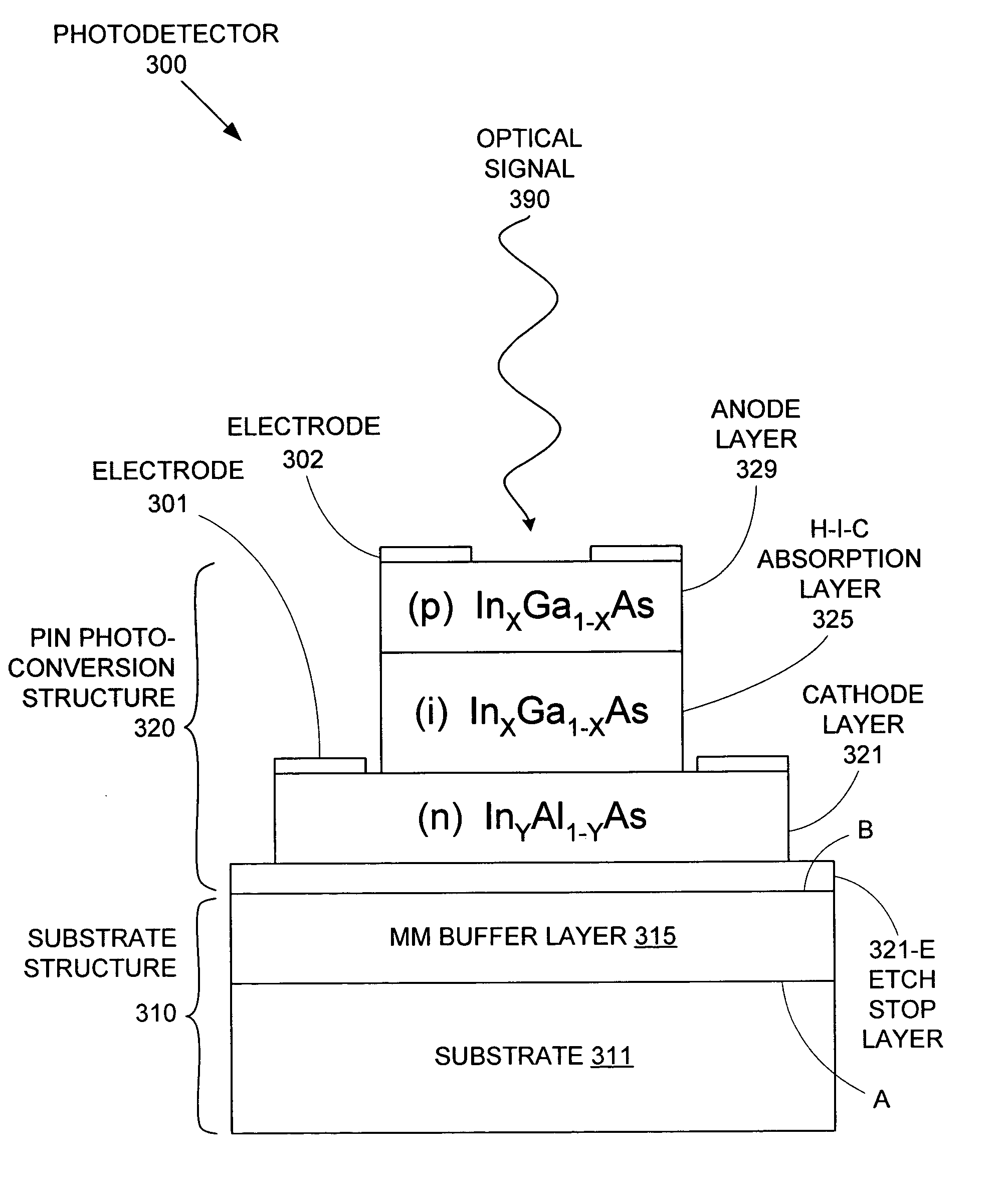
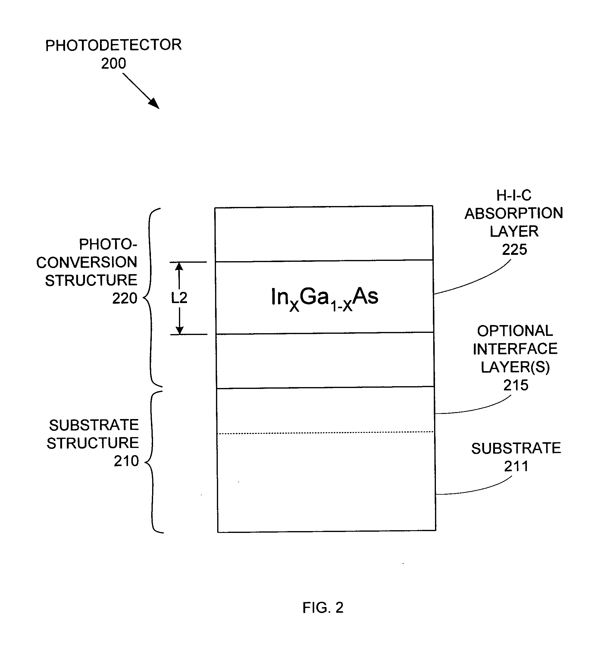
FIG. 2 shows a cross-section of a photodetector 200 in accordance with an embodiment of the invention. Photodetector 200 includes a photoconversion structure 220 on a substrate structure 210. Photoconversion structure 220 performs the optical-to-electrical signal conversion, and includes a high-indium-concentration (H-I-C) absorption layer 225 formed from InGaAs. Specifically, H-I-C absorption layer 225 is formed from an InxGa1-xAs layer, where X is between 0.53 and 1.0. That is, the Group III sublattice concentration of indium is greater than 53% and less than 100%.
H-I-C absorption layer 225 is typically a non-intentionally doped (NID) layer. Note that photoconversion structure 220 can comprise any type of photoconversion structure (e.g., PIN (mesa-based or planar-diffused), dual path PIN, waveguide PIN, RCE, avalanche (also mesa-based or planar-diffused), and MSM photodiodes). Note further that substrate structure 210 can comprise an optional interface layer(s) 215 that accommoda...
PUM
 Abstract
Description
Claims
Application Information