
Lateral type photodiode, image sensor including the same, and method of manufacturing the photodiode and the image sensor.

Active Publication Date: 2015-11-19
SAMSUNG ELECTRONICS CO LTD
View PDF3 Cites 7 Cited by
  • Summary
  • Abstract
  • Description
  • Claims
  • Application Information

AI Technical Summary

Benefits of technology

The patent text describes methods for increasing the light receiving area of a photodiode in an image sensor. The methods involve forming an insulation mask layer with a through hole and growing semiconductor layers in a way that increases the ratio of light receiving area to the size of the photodiode. This allows for a larger light sensing area, which can improve the performance of the image sensor. The methods can be used in the manufacturing of both lateral type photodiodes and image sensors with the active layer and second type semiconductor layers sequentially disposed. The technical effect of the patent text is to provide a method for increasing the light sensing area of a photodiode in an image sensor.

Problems solved by technology

Thus, a number of complicated manufacturing processes are used, and it is often difficult to align the photodiode and the readout circuit.
Moreover, since it is difficult to reduce a size of the readout circuit, a ratio of the light receiving area in the pixel is gradually reduced as the pixel size is reduced.

Method used


Image

  • Lateral type photodiode, image sensor including the same, and method of manufacturing the photodiode and the image sensor.
  • Lateral type photodiode, image sensor including the same, and method of manufacturing the photodiode and the image sensor.
  • Lateral type photodiode, image sensor including the same, and method of manufacturing the photodiode and the image sensor.

Examples


Embodiment Construction

[0056]Reference will now be made in detail to example embodiments, examples of which are illustrated in the accompanying drawings, wherein like reference numerals refer to like elements throughout. In this regard, the example embodiments may have different forms and should not be construed as being limited to the descriptions set forth herein. Accordingly, the example embodiments are merely described below, by referring to the figures, to explain the present description. Expressions such as “at least one of,” when preceding a list of elements, modify the entire list of elements and do not modify the individual elements of the list.

[0057]It will be understood that when an element is referred to as being “on,”“connected” or “coupled” to another element, it can be directly on, connected or coupled to the other element or intervening elements may be present. In contrast, when an element is referred to as being “directly on,”“directly connected” or “directly coupled” to another element, ...


PUM


Abstract

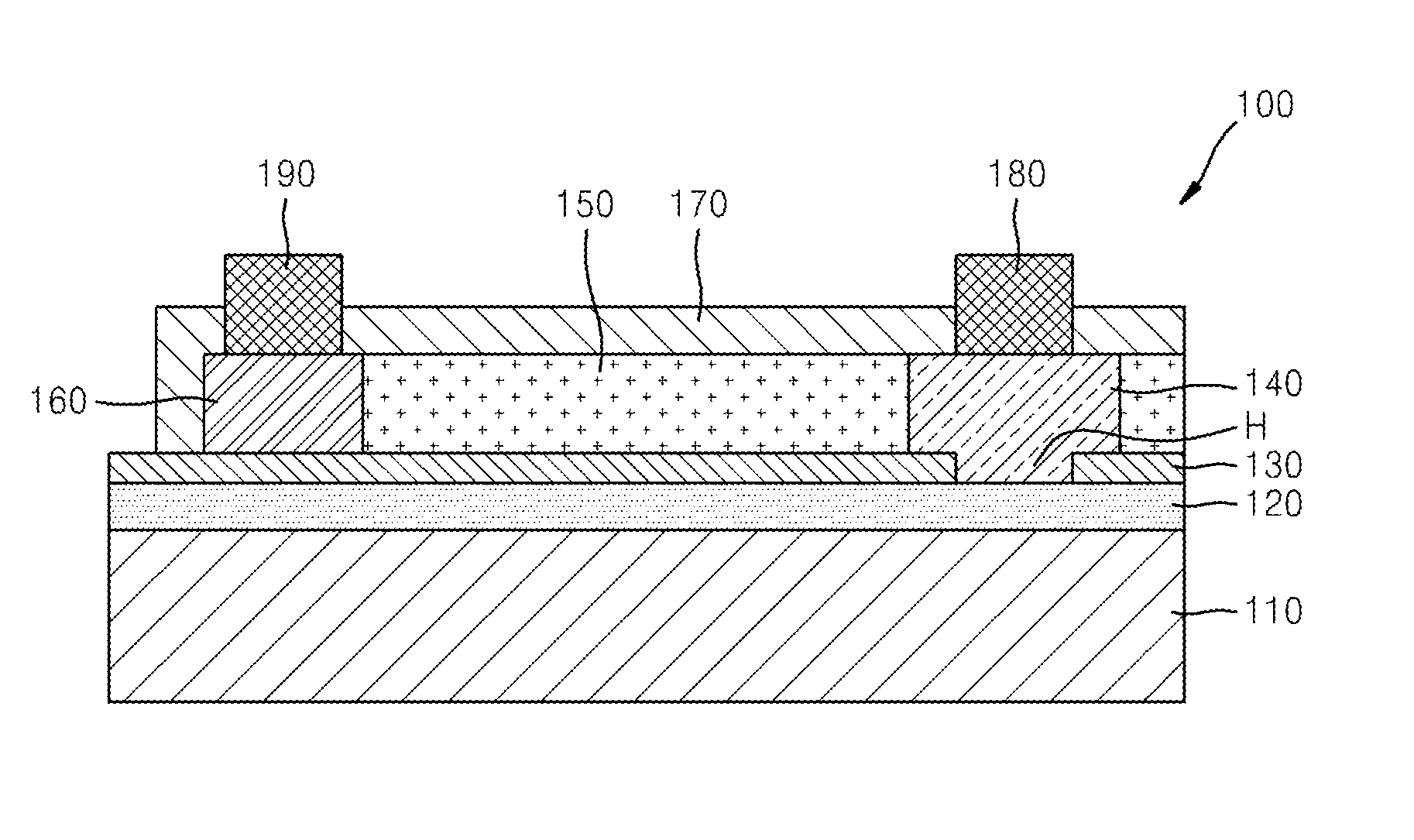
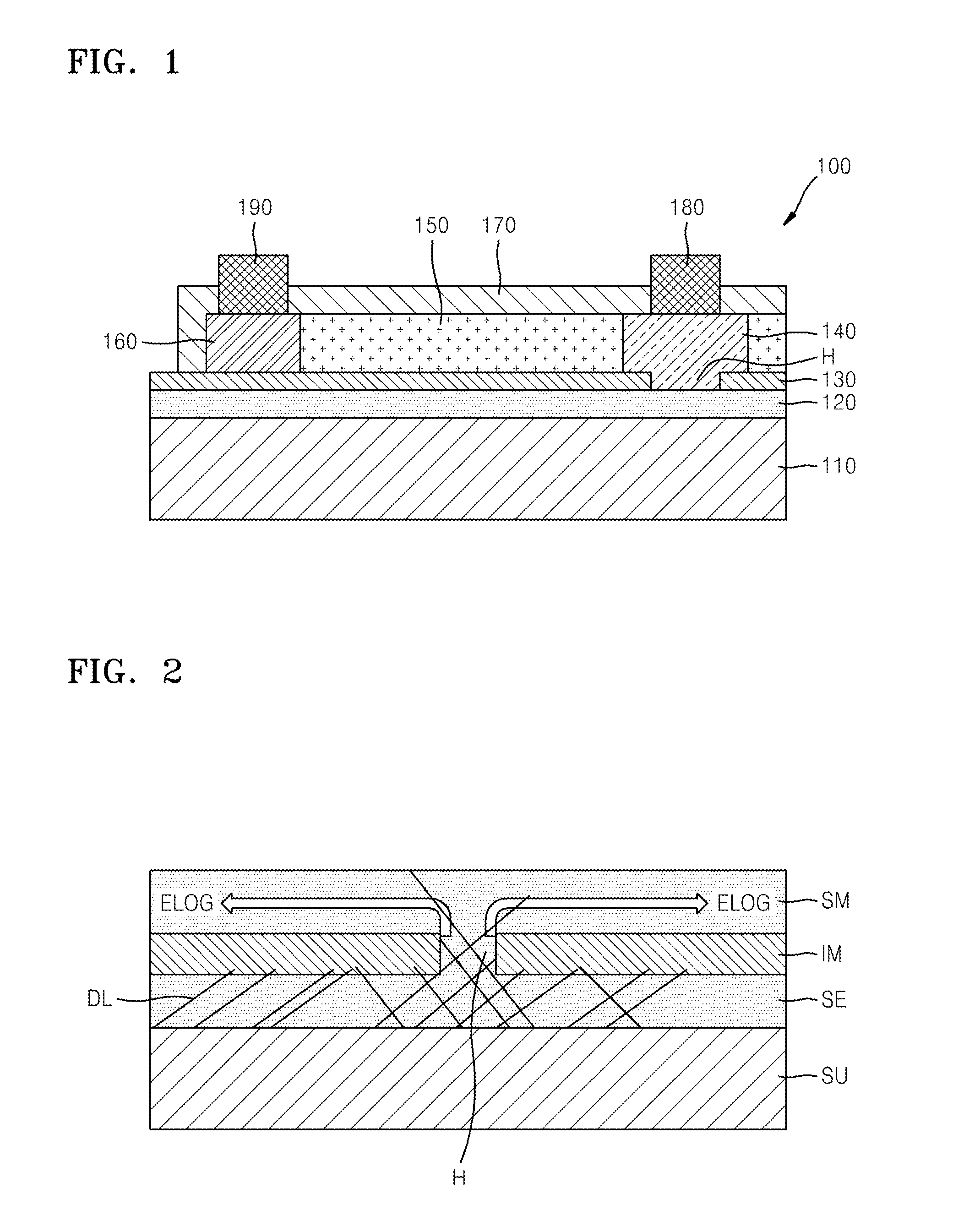
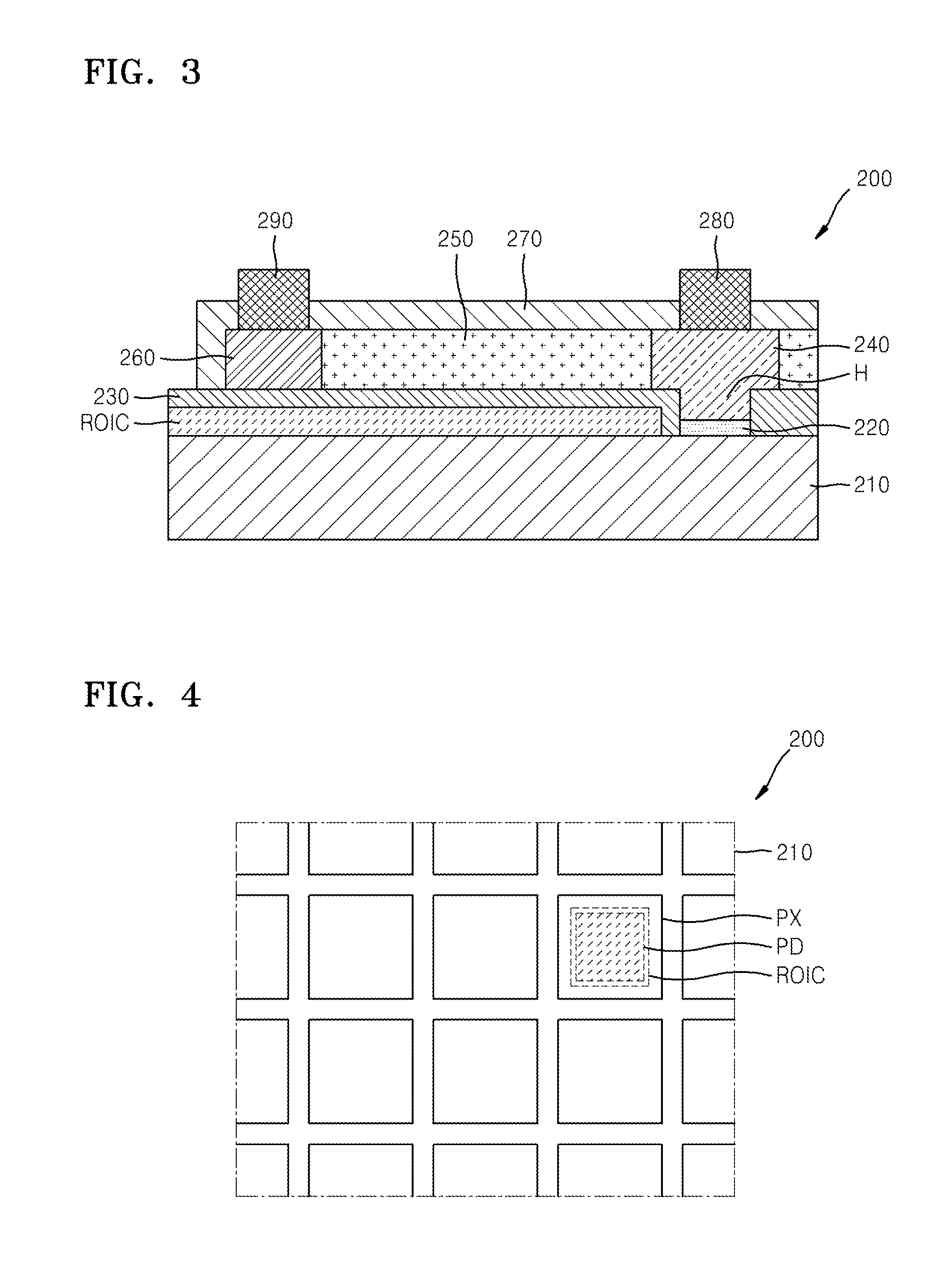
Example embodiments relate to a lateral type photodiode including a substrate, an insulation mask layer formed on the substrate, and a first type semiconductor layer, an active layer, and a second type semiconductor layer that contact a surface of the insulation mask layer and that are sequentially disposed in a direction substantially parallel to the surface of the insulation mask layer. The insulation mask layer includes a through hole, and the first type semiconductor layer, the active layer, and the second type semiconductor layer are sequentially formed from the through hole by using a lateral overgrowth method.

Description

RELATED APPLICATION[0001]This application claims the benefit of priority from Korean Patent Application No. 10-2014-0057952, filed on May 14, 2014, in the Korean Intellectual Property Office, the disclosure of which is incorporated herein in its entirety by reference.BACKGROUND[0002]1. Field[0003]Example embodiments relate to group III-V compound semiconductor-based photodiodes, image sensors including the photodiodes, and / or methods of manufacturing the photodiodes and the image sensors.[0004]2. Description of the Related Art[0005]An image sensor is a semiconductor device that converts an optical image to an electrical signal and that is typically used in various fields such as cameras, motion recognition cameras, and touch panels.[0006]The image sensor includes a light receiving element that senses light and converts the light to an electrical signal and a readout circuit that processes the electrical signal to form the same to data.[0007]A photodiode based on a group III-V compou...

Claims


Application Information

Patent Timeline
IPC IPC(8): H01L31/0352H01L31/0336H01L31/18H01L31/105
CPCH01L31/035281H01L31/1852H01L31/0336H01L31/105H01L31/03529H01L31/184H01L27/14601H01L27/14643Y02E10/544Y02P70/50H01L31/0352H01L31/18
Inventor AHN, JIHOONJEON, YONGWOOKIM, JUNGWOOPARK, HAESEOKAHN, SEUNGEONLEE, SEUNGHYUPJUNG, MYOUNGHOONCHOI, HYUKSOON
Owner SAMSUNG ELECTRONICS CO LTD
Learn More