TFT array substrate, display panel and display device

a technology of array substrate and display panel, applied in static indicating devices, instruments, time-delay networks, etc., can solve the problems of low yield, high power consumption, and low yield of display devices

Active Publication Date: 2015-11-26
WUHAN TIANMA MICRO ELECTRONICS CO LTD +1
View PDF3 Cites 16 Cited by
  • Summary
  • Abstract
  • Description
  • Claims
  • Application Information

AI Technical Summary

Benefits of technology

[0017]It is further found by the researchers that both the triggering signal and the reset signal are pulse signals and both are regular in their phase cycles. If a pulse signal (e.g. a triggering signal) applied to a clock signal terminal is reused as a reset signal applied to a reset terminal, then resetting signal lines individually providing reset signals can be omitted, so that the amount of signal lines can be reduced and corresponding beneficial effects can also be obtained.

Problems solved by technology

In practice, however, it is found that the display device has problems such as high power consumption, a high cost, a low yield, and a large border width.

Method used


Image

  • TFT array substrate, display panel and display device
  • TFT array substrate, display panel and display device
  • TFT array substrate, display panel and display device

Examples


Embodiment Construction

[0015]In order to make the above objects, features and advantages of the present disclosure more clear and apparent, specific embodiments of the present disclosure are illustrated in detail below in combination with the accompanying drawings.

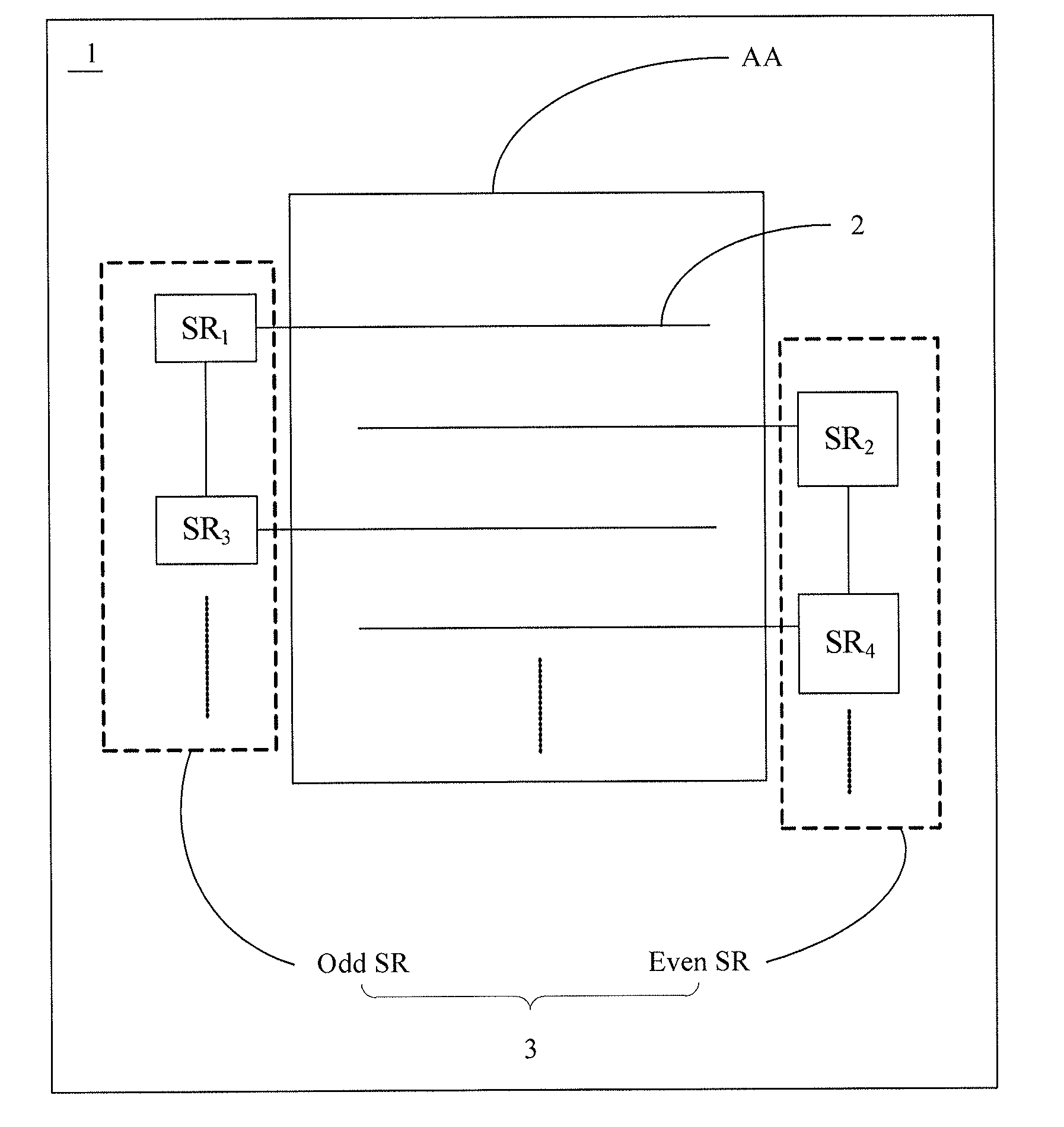
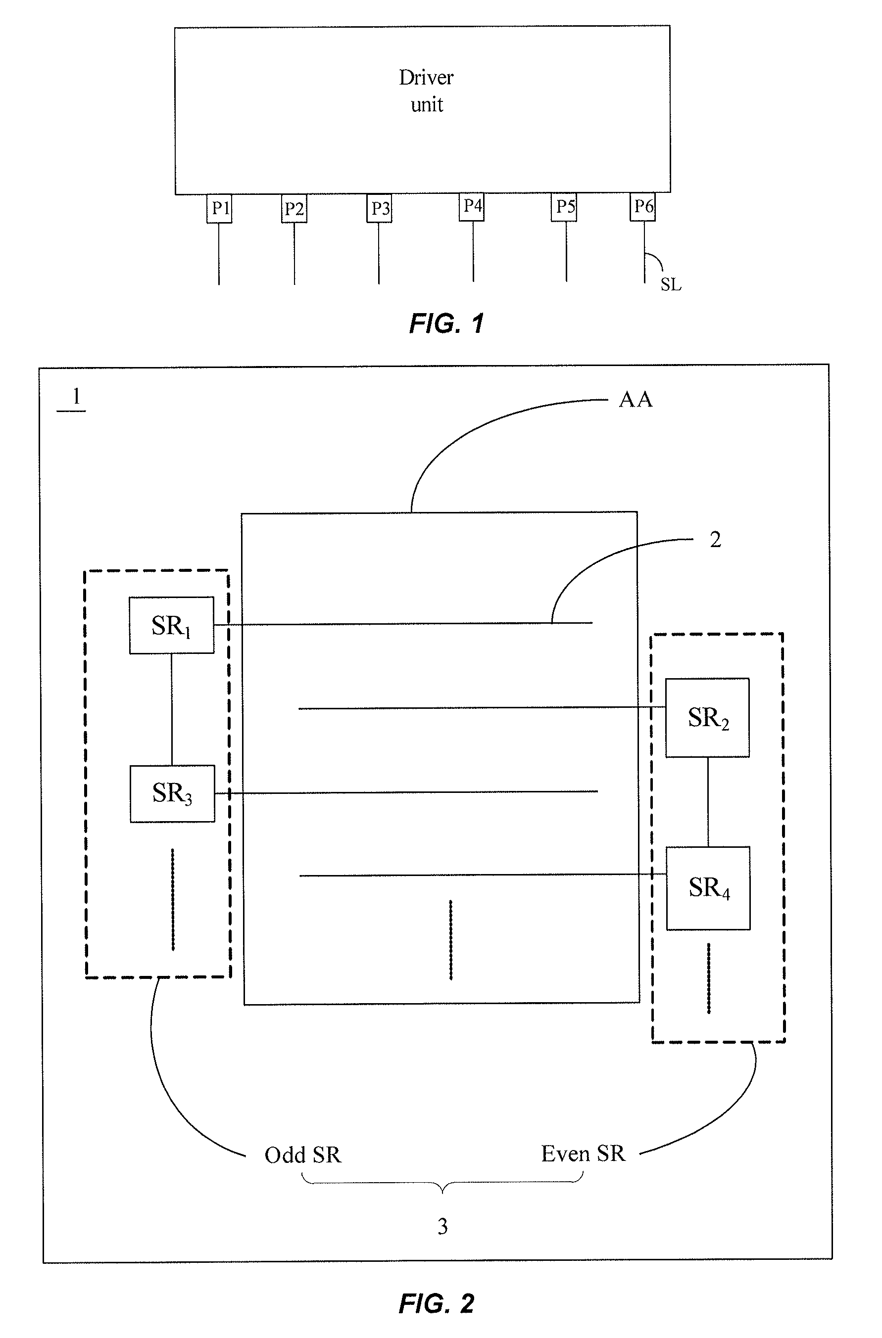
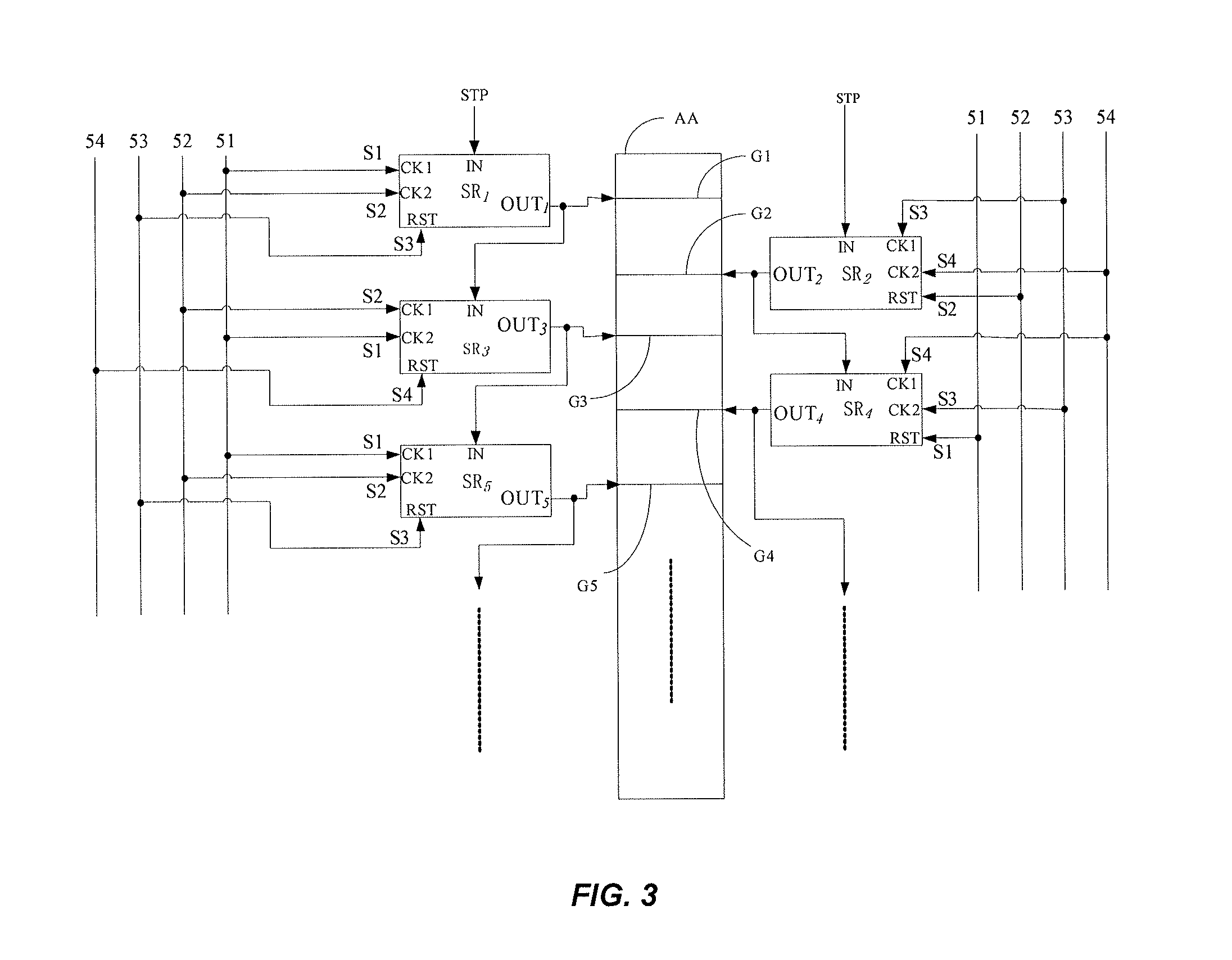
[0016]It has been found by researchers that problems of existing display devices such as high power consumption, a high cost, a low yield, and a large border width are caused by following reasons: as shown in FIG. 1, excessive signal lines (generally including six signal lines (SLs), i.e. three triggering signal lines and three resetting signal lines, where the three triggering signal lines are configured to sequentially trigger three consecutive odd-numbered stages of shift registers; and the three resetting signal lines are configured to sequentially reset three consecutive odd-numbered stages of shift registers; or, the three triggering signal lines are configured to sequentially trigger three consecutive even-numbered stages of shift registe...


PUM

PropertyMeasurementUnit
temperatureaaaaaaaaaa
phase differenceaaaaaaaaaa
structureaaaaaaaaaa

Abstract

A TFT array substrate is disclosed. The TFT array substrate includes a plurality of gate lines, and a gate driving circuit connected to the gate lines. The gate driving circuit includes a plurality of stages of shift registers, where odd-numbered stages of shift registers are cascaded-connected to each other, even-numbered stages of shift registers are cascaded-connected to each other, and the odd-numbered stages of shift registers and the even-numbered stages of shift registers are disposed at opposite ends of the gate lines.

Description

CROSS-REFERENCES TO RELATED APPLICATIONS[0001]This application claims the benefit of priority to Chinese Patent Application No. 201410217830.X, filed with the Chinese Patent Office on May 21, 2014 and entitled “TFT ARRAY SUBSTRATE, DISPLAY PANEL AND DISPLAY DEVICE”, the content of which is incorporated herein by reference in its entirety.TECHNICAL FIELD[0002]The present disclosure relates to the field of display technologies, in particular to a TFT array substrate, a display panel and a display device.BACKGROUND OF THE INVENTION[0003]Currently, a display device has been used in increasing applications. In practice, however, it is found that the display device has problems such as high power consumption, a high cost, a low yield, and a large border width.BRIEF SUMMARY OF THE INVENTION[0004]One inventive aspect is a TFT array substrate. The TFT array substrate includes a plurality of gate lines, and a gate driving circuit connected to the gate lines. The gate driving circuit includes ...

Claims


Application Information

Patent Timeline
Patent Type & Authority Applications(United States)
IPC IPC(8): G11C27/04H01L27/12G09G3/20G09G3/3225
CPCG11C27/04G09G3/2092H01L27/124G09G2330/021G09G2310/0286G09G2300/0465H01L27/1255G09G3/3677G09G2300/0417G09G2300/0426G09G2310/0224G09G2310/061G11C19/184G11C19/28
Inventor QIAN, DONG
Owner WUHAN TIANMA MICRO ELECTRONICS CO LTD
Why Eureka
Try Eureka