Flat panel display having low reflective black matrix and method for manufacturing the same

a flat panel display and black matrix technology, applied in the field of flat panel displays, can solve the problems of affecting the observation feeling and quality of users, affecting the overall light transmissivity, and affecting the quality of video, so as to reduce the reflective light, prevent light reflection, and low reflective property

Active Publication Date: 2015-11-26
LG DISPLAY CO LTD
View PDF25 Cites 25 Cited by
  • Summary
  • Abstract
  • Description
  • Claims
  • Application Information

AI Technical Summary

Benefits of technology

[0026]An object of the present invention is to provide a flat panel display without a polarization sheet or plate for preventing light reflection and a method for manufacturing the same.
[0027]Another object of the present invention is to provide a flat panel display comprising a low reflective black matrix for reducing the reflective light by the black matrix d...

Problems solved by technology

Therefore, lights incident from the outside may be reflected by outside surface of the lower substrate SUB or the encap substrate ENC so that the reflective light may hinder the observation feeling and quality of the user.
Especially, in the case that black matrix are disposed between each pixel, the light may ...

Method used


Image

  • Flat panel display having low reflective black matrix and method for manufacturing the same
  • Flat panel display having low reflective black matrix and method for manufacturing the same
  • Flat panel display having low reflective black matrix and method for manufacturing the same

Examples


first embodiment

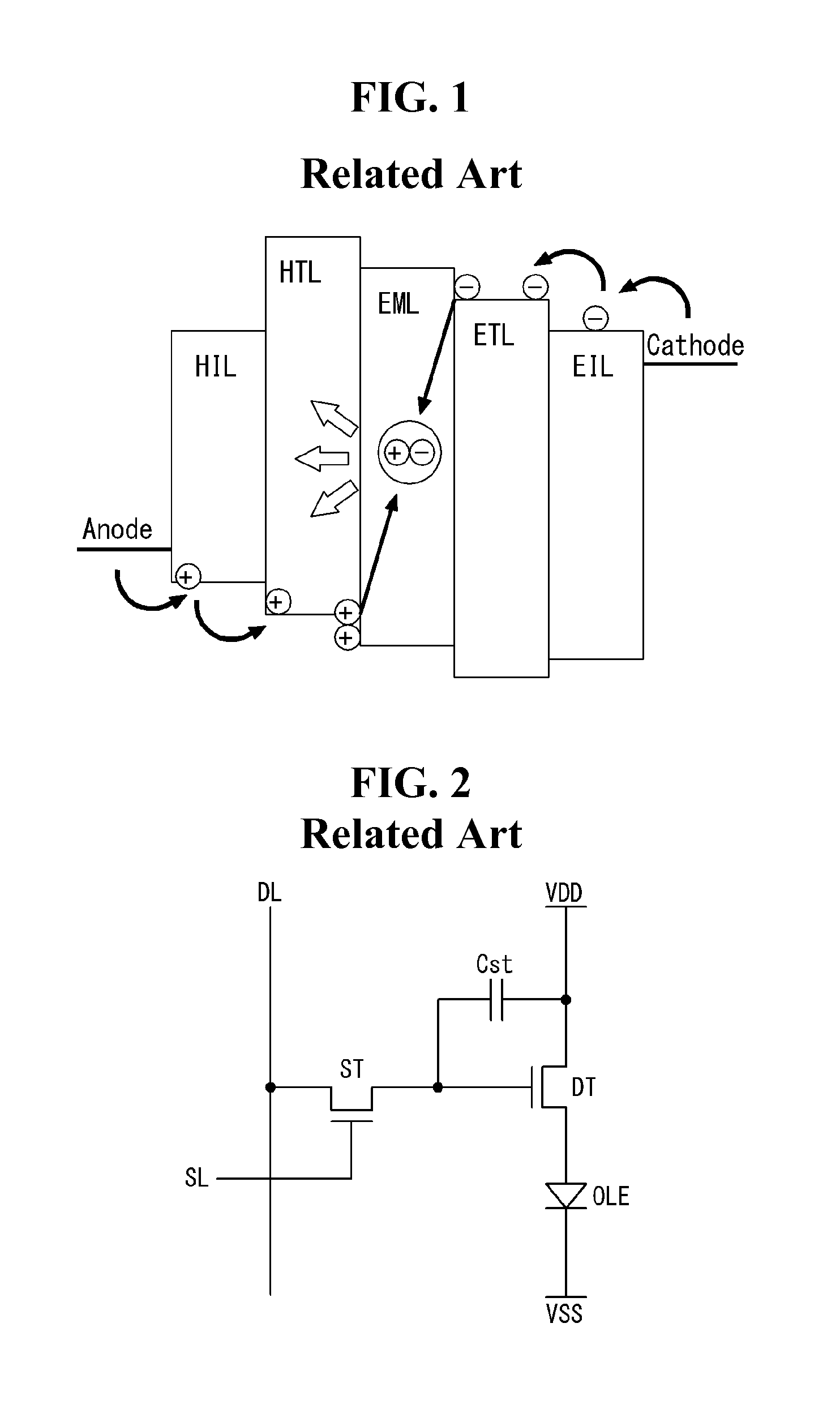
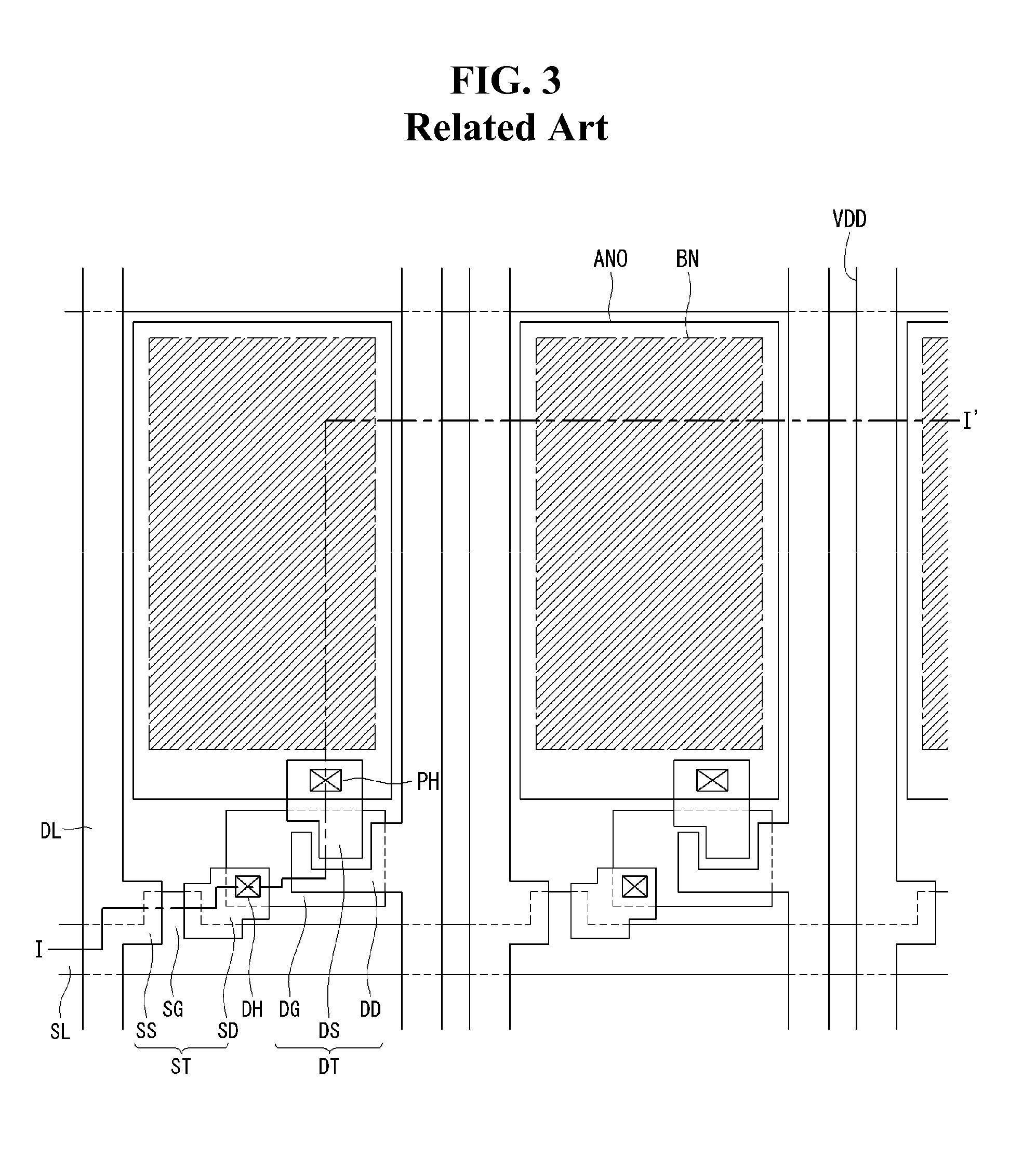
[0047]A bottom emission type organic light emitting diode display according to the present disclosure has a plurality of pixel areas disposed on a substrate SUB in a matrix manner. Each pixel area includes an open area AA where an organic light emitting diode for representing the pixel data into video information is formed, and a non-open area NA where various elements for driving the organic light emitting diode is disposed.

[0048]On the substrate SUB, gate electrodes SG and DG for a switching thin film transistor ST and a driving thin film transistor DT, respectively are formed. On the gate electrodes SG and DG, a gate insulating layer GI is deposited. On some portions of the gate insulating layer GI overlapping with the gate electrodes SG and DG, semiconductor layer SA and DA are formed. On the semiconductor layers SA and DA, source electrodes SS and DS and drain electrodes SD and DD which are facing and apart from each other with a predetermined distance, respectively, are formed...

second embodiment

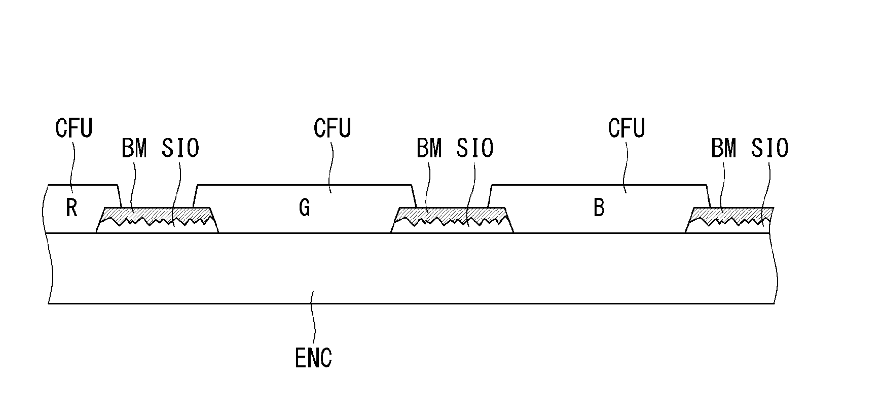
[0067]Further, in the second embodiment, in order to enhance the color purity, an upper color filter CFU may be further included at the inner surface of the encap substrate ENC. It is preferable that the upper color filter CFU may be disposed as being overlapped with the lower color filter CFL exactly.

[0068]For the top emission type organic light emitting diode display, the user sees or observes the video information at the outer side of the encap substrate ENC. A black matrix BM may be further included on the inner surface of the encap substrate ENC facing the user, and the black matrix BM is covering the non-open area NA. The black matrix BM can prevent from the color distortion by mixing of the neighboring two colors (i.e. red and green or green and blue).

[0069]For example, it is preferable that the black matrix BM is made of black material. However, all black material has some reflective property, even though it is a low degree. Therefore, out light may be reflected by the black...


PUM


Abstract

A flat panel display having a low reflective black matrix and a method for manufacturing the same are provided. The flat panel display includes a substrate having an open area and a non-open area; a hazy layer disposed in the non-open area on the inner surface of the substrate; a black matrix stacked on the hazy layer; a driving element disposed in the non-opening area; and a display element disposed in the open area and driven by the driving element.

Description

[0001]This application claims the benefit of Korea Patent Application No. 10-2014-0061756 filed on May 22, 2014, which is incorporated herein by reference for all purposes as if fully set forth herein.BACKGROUND OF THE INVENTION[0002]1. Field of the Invention[0003]The present disclosure relates to a flat panel display, and more particularly, to a flat panel display having a low reflective black matrix and a method for manufacturing the same.[0004]2. Discussion of the Related Art[0005]Nowadays, various flat panel display devices are developed for overcoming many drawbacks of the cathode ray tube such as heavy weight and bulk volume. The flat panel display devices include the liquid crystal display device (or LCD), the field emission display (or FED), the plasma display panel (or PDP) and the electroluminescence device (or EL). Especially, a high quality flat panel display adopting the low temperature poly silicon (or, LTPS) as the channel device is increasingly required.[0006]The ele...

Claims


Application Information

Patent Timeline
IPC IPC(8): H01L27/32H01L51/56H01L51/52
CPCH01L27/3244H01L27/322H01L51/5284H01L51/5268H01L2227/323H01L51/56H01L2251/303H01L2251/301H01L2251/558H01L51/5271H10K59/38H10K59/12H10K50/865H10K50/854H10K50/856H10K71/00H10K59/1201H10K2102/00H10K2102/351
Inventor LEE, JINBOKKIM, YONGILLEE, EUNHYE
Owner LG DISPLAY CO LTD
Why Eureka
Try Eureka