
Eureka
For R&D, Eureka makes reading and utilizing patents & technical documents easy.
Eureka AIR
Designed for self-driven R&D workflows. Generate viable solutions, solve complex R&D challenges, empower your innovation with AI.

Eureka Materials
Designed for material experts only. Revolutionize your material R&D, from search, analyze, to developing new materials.

TechResearch
Generate reliable direction feasibility study reports for your R&D in just a few steps.

TechSeek
Discover and master advanced knowledge NOW. Basics, ideas, possibilities, all at once.

TechMind
As an expert in R&D Theories, TechMind can generates customized viable solutions instantly.

TechRisk
Analyze your overall solution with one click, know your potential R&D risks in advance.

TechMonitor
Get weekly tech updates, stay abreast of the latest tech innovations and key insights.
Anisotropic Magnetoresistive Device and Method for Fabricating the Same
- Summary
- Abstract
- Description
- Claims
- Application Information
AI Technical Summary
Benefits of technology
Problems solved by technology
Method used
Image

Examples
first embodiment
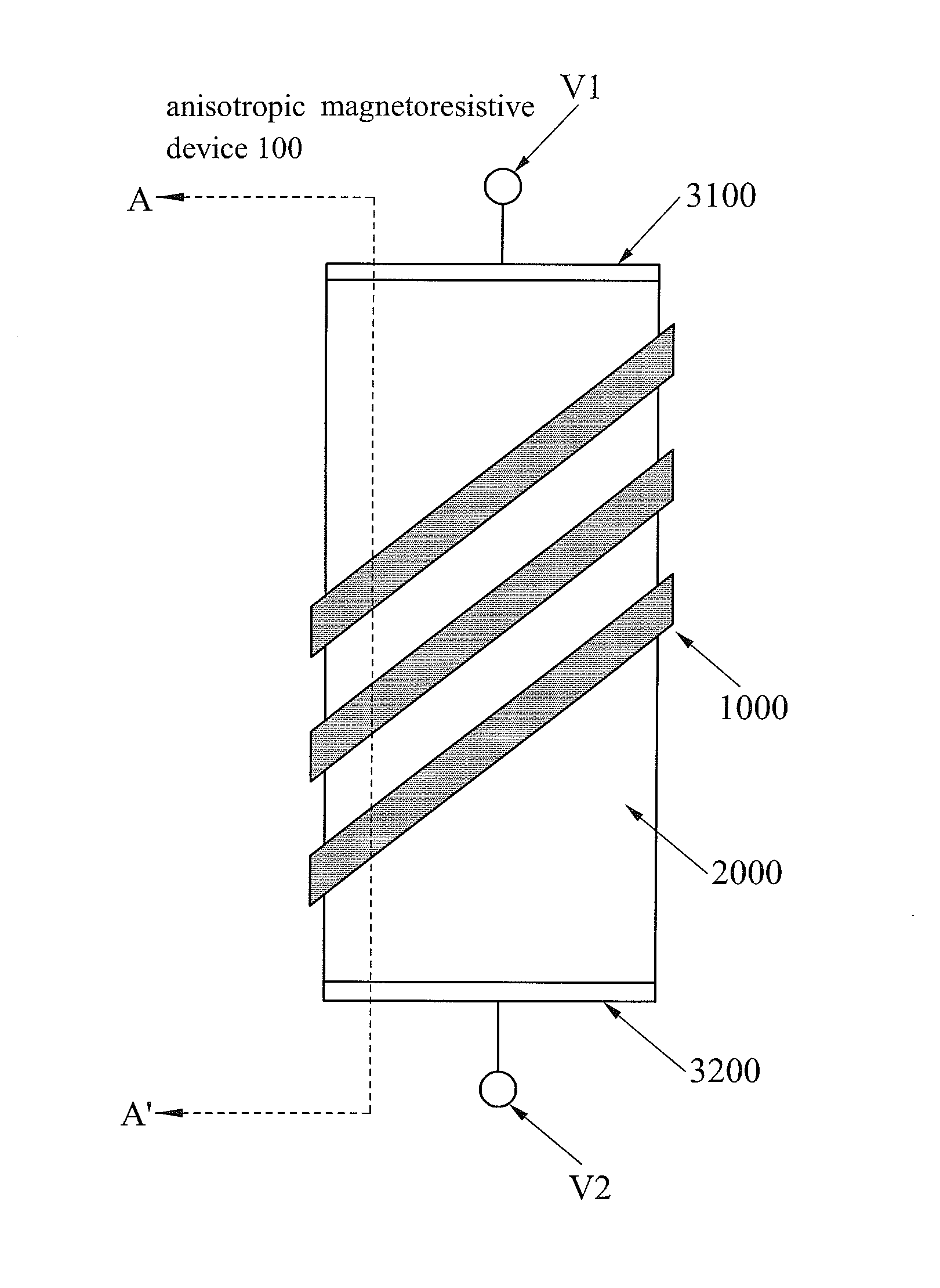
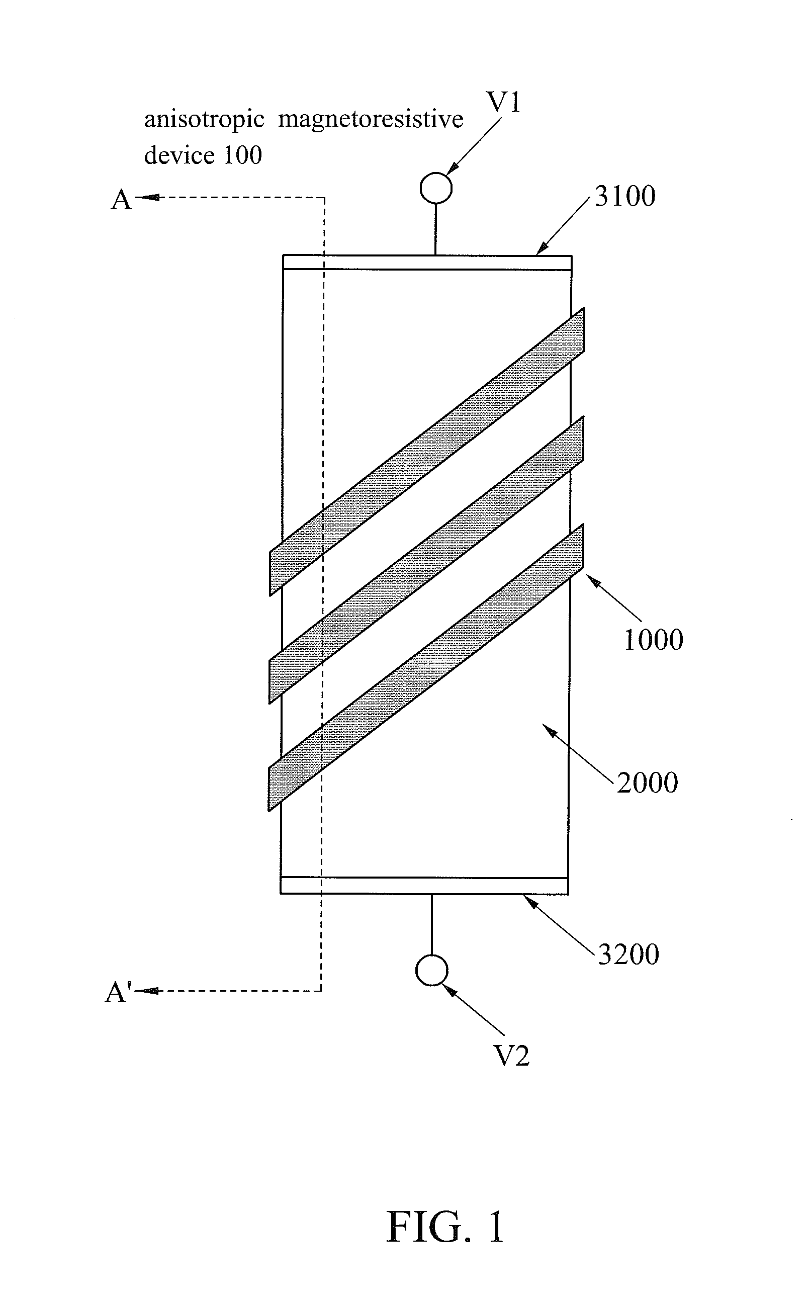
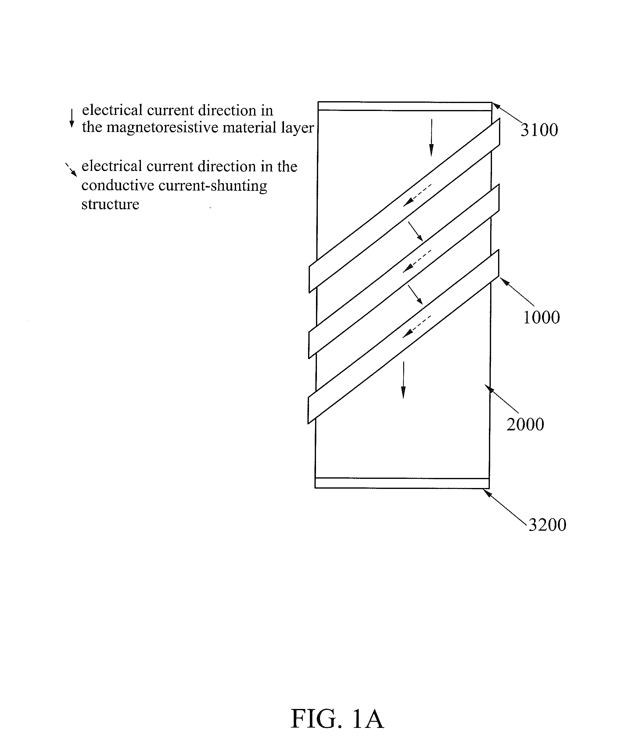
[0039]Now please refer to FIG. 1 and FIG. 2. FIG. 1 shows the schematic diagram illustrating the anisotropic magnetoresistive device 100 according to one embodiment of the present invention. FIG. 2 shows the schematic cross-sectional view of the anisotropic magnetoresistive device 100 taken along line A-A′ of FIG. 1 according to the present invention. FIG. 1 focuses on the shape and orientation of each element of the anisotropic magnetoresistive device 100. FIG. 2 focuses on the relative locations of each element of the anisotropic magnetoresistive device 100 and environmental elements around the device 100. In FIG. 1, it is clear that the anisotropic magnetoresistive device 100 capable of sensing an external magnetic field of a direction mainly comprises a magnetoresistive material layer 2000, a conductive current-shunting structure 1000 and electrodes 3100 and 3200.
[0040]The magnetoresistive material layer 2000 can be designed to be a long strip disposed above the surface of a sub...
second embodiment
[0048]Now please refer to FIG. 3. FIG. 3 shows the schematic cross-sectional view of the anisotropic magnetoresistive device 100 taken along line A-A′ of FIG. 1 according to the present invention. In order to understand the relative locations of each element of the anisotropic magnetoresistive device 100 and environmental elements around the device 100, in FIG. 3, lower portion 30*, middle portion 20* and upper portion 10* are defined in a wafer from bottom to top. The lower portion 30* is similar to the lower portion 30 of FIG. 2, so its detail is omitted to avoid repetition. The middle portion 20* is similar to the middle portion 20 of FIG. 2 and comprises inter-metal dielectric layers IMD1-IMDx−1 and most of the interconnect structure (metal wiring layers M1-Mx−1 and metal via layers V1-Vx−1 in this embodiment), wherein x is an integer equal to or greater than 3. The upper portion 10* is different from the upper portion 10 and comprises inter-metal dielectric layer IMDx and IMDx+...
third embodiment
[0052]No please refer to FIG. 4. FIG. 4 shows the schematic cross-sectional view of the anisotropic magnetoresistive device 100 taken along line A-A′ of FIG. 1 according to the present invention. In order to understand the relative locations of each element of the anisotropic magnetoresistive device 100 and environmental elements around the device 100, lower portion 31, middle portion 21 and upper portion 11 are defined in a wafer from bottom to top. The lower portion 31 is similar to the lower portion 30 of FIG. 2 in terms of its components and manufacturing method, so its detail would be omitted. The middle portion 21 is similar to the middle portion 20 of FIG. 2 and comprises inter-metal dielectric layers IMD1-IMDx−1 and most of the interconnect structure (metal wiring layers M1-Mx−1 and metal via layers V1-Vx−1), wherein x is an integer equal to or greater than 3. The upper portion 11 is similar to the upper portion 10 of FIG. 2 and comprises the inter-metal dielectric layer IMD...
PUM
 Abstract
Description
Claims
Application Information
 - R&D Engineer
- R&D Manager
- IP Professional
- Industry Leading Data Capabilities
- Powerful AI technology
- Patent DNA Extraction
Browse by: Latest US Patents, China's latest patents, Technical Efficacy Thesaurus, Application Domain, Technology Topic, Popular Technical Reports.
© 2024 PatSnap. All rights reserved.Legal|Privacy policy|Modern Slavery Act Transparency Statement|Sitemap|About US| Contact US: help@patsnap.com