

Organic electroluminescent element
a technology of electroluminescent elements and organic materials, which is applied in the direction of luminescent compositions, organic chemistry, thiazine dyes, etc., can solve the problems of improving efficiency and problematic fluorescence emission, and achieve the effect of long li
- Summary
- Abstract
- Description
- Claims
- Application Information
AI Technical Summary
Benefits of technology
Problems solved by technology
Method used
Image

Examples
first exemplary embodiment
Arrangement(s) of Organic EL Device
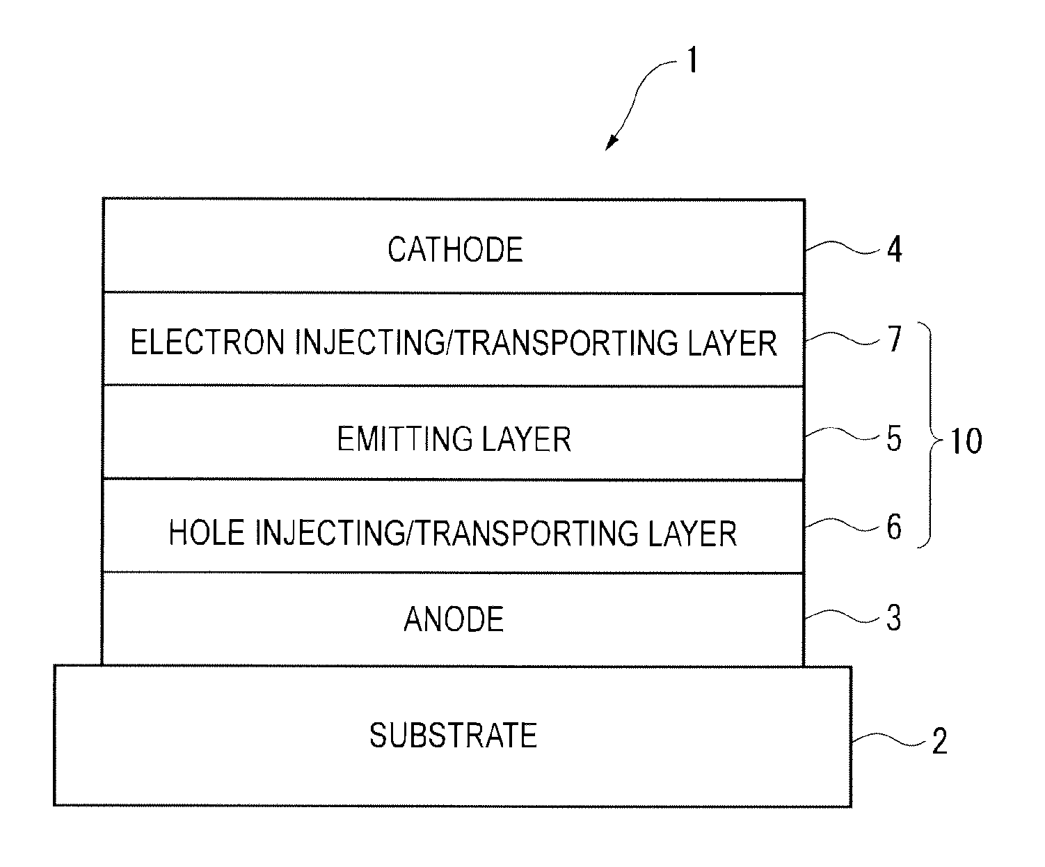
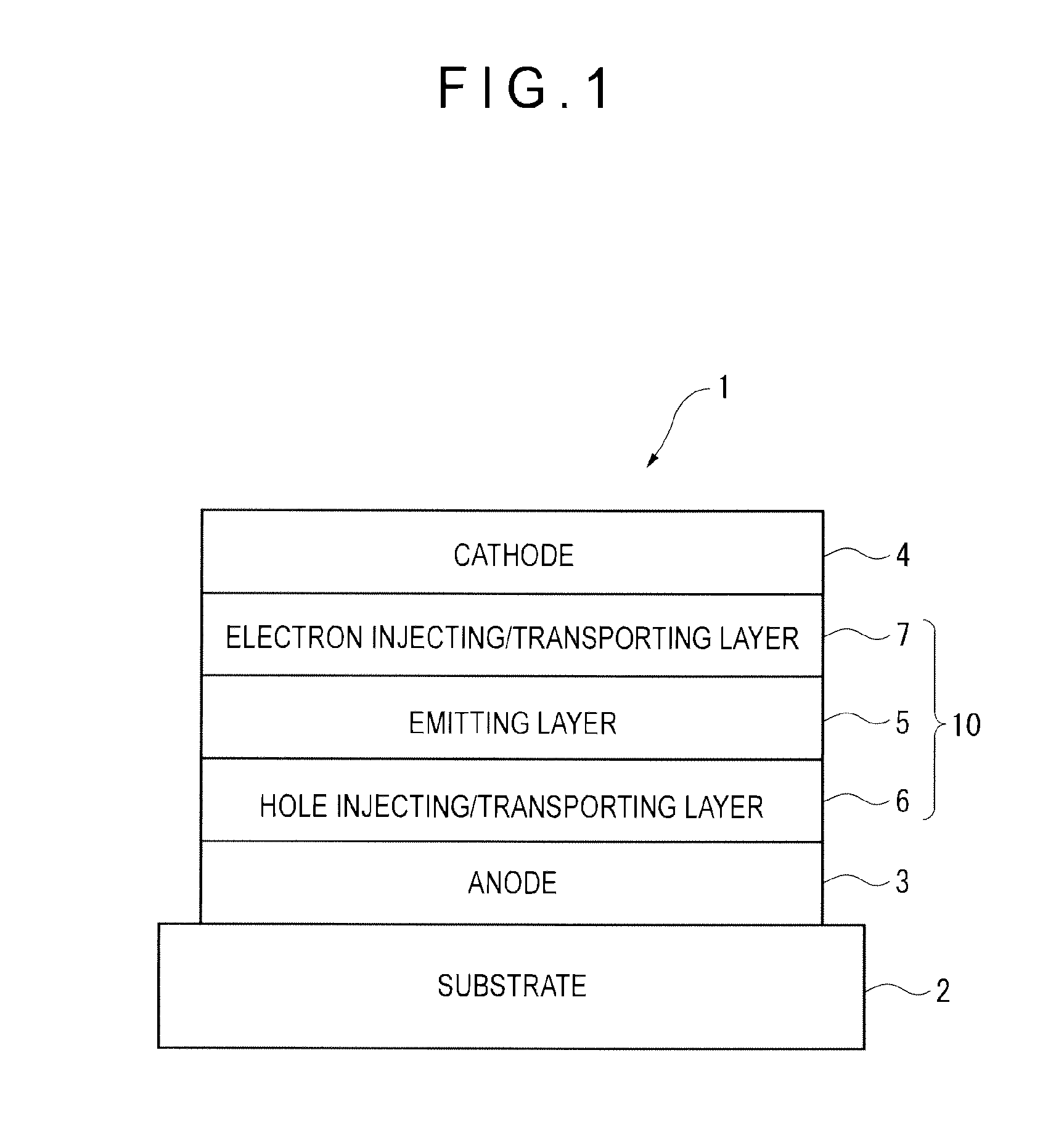
[0019]An organic EL device according to a first exemplary embodiment of the invention will be described below.
[0020]The organic EL device in the first exemplary embodiment includes a pair of electrodes and an organic layer between the pair of electrodes. The organic layer includes at least one layer formed of an organic compound. The organic layer may further include an inorganic compound.
[0021]In the organic EL device in the exemplary embodiment, at least one layer of the organic layer(s) is the emitting layer. Accordingly, the organic layer may be provided by a single emitting layer. Alternatively, the organic layer may be provided by layers employed in an organic EL device such as a hole injecting layer, a hole transporting layer, an electron injecting layer, an electron transporting layer, a hole blocking layer, and an electron blocking layer.
[0022]The following are representative structure examples of an organic EL device:
(a) anode / emitting la...
second exemplary embodiment
[0257]An organic EL device according to a second exemplary embodiment will be described below. In the description of the second exemplary embodiment, the same components as those in the first exemplary embodiment are denoted by the same reference signs and names to simplify or omit an explanation of the components. In the second exemplary embodiment, the same materials and compounds as described in the first exemplary embodiment are usable for a material and a compound which are not particularly described.
[0258]The organic EL device in the second exemplary embodiment has the same device arrangement as in the first exemplary embodiment, in which the compounds contained in the emitting layer are different. The organic EL device 1 in the second exemplary embodiment contains the first and second compounds according to the first exemplary embodiment and a third compound in the emitting layer. The third compound is also a compound emitting thermally activated delayed fluorescence. Also in...
third exemplary embodiment
[0266]An organic EL device according to a third exemplary embodiment will be described below. In the description of the second exemplary embodiment, the same components as those in the first exemplary embodiment are denoted by the same reference signs and names to simplify or omit an explanation of the components. In the third exemplary embodiment, the same materials and compounds as described in the above exemplary embodiments are usable for a material and a compound which are not particularly described.
[0267]The thermally activated delayed fluorescence compound is exemplified by a compound represented by a formula (2) below. In the third exemplary embodiment, one of the thermally activated delayed fluorescence compounds contained in the emitting layer is represented by the formula (2) below. The compound represented by the formula (1) described in the above exemplary embodiments may also be used as the thermally activated delayed fluorescence compound.
[0268]In the formula (2), L20...
PUM
 Abstract
Description
Claims
Application Information