Expansion method, method for manufacturing semiconductor device, and semiconductor device

a semiconductor device and expansion method technology, applied in semiconductor devices, semiconductor/solid-state device details, electrical devices, etc., can solve the problems of minute defects (also referred to as “chipping”) on semiconductor chips, damage to circuit patterns, and the problem of chipping becoming more critical, so as to achieve favorable cutting and efficient manufacturing of semiconductor devices

Active Publication Date: 2015-12-03
RESONAC CORP
View PDF3 Cites 63 Cited by
  • Summary
  • Abstract
  • Description
  • Claims
  • Application Information

AI Technical Summary

Benefits of technology

[0018]One embodiment of the present invention is able to provide an expansion method that enables a semiconductor wafer and a die bonding film to be cut favorably. Further, other embodiments of the present inv

Problems solved by technology

In the blade cutting method, minute defects (also referred to as “chipping”) are sometimes formed on the semiconductor chip as a result of the cutting resistance generated during the cutting process.
This occurrence of chipping not only impairs the external appearance of the semiconductor chip, but depending on the de

Method used


Image

  • Expansion method, method for manufacturing semiconductor device, and semiconductor device
  • Expansion method, method for manufacturing semiconductor device, and semiconductor device
  • Expansion method, method for manufacturing semiconductor device, and semiconductor device

Examples


first embodiment

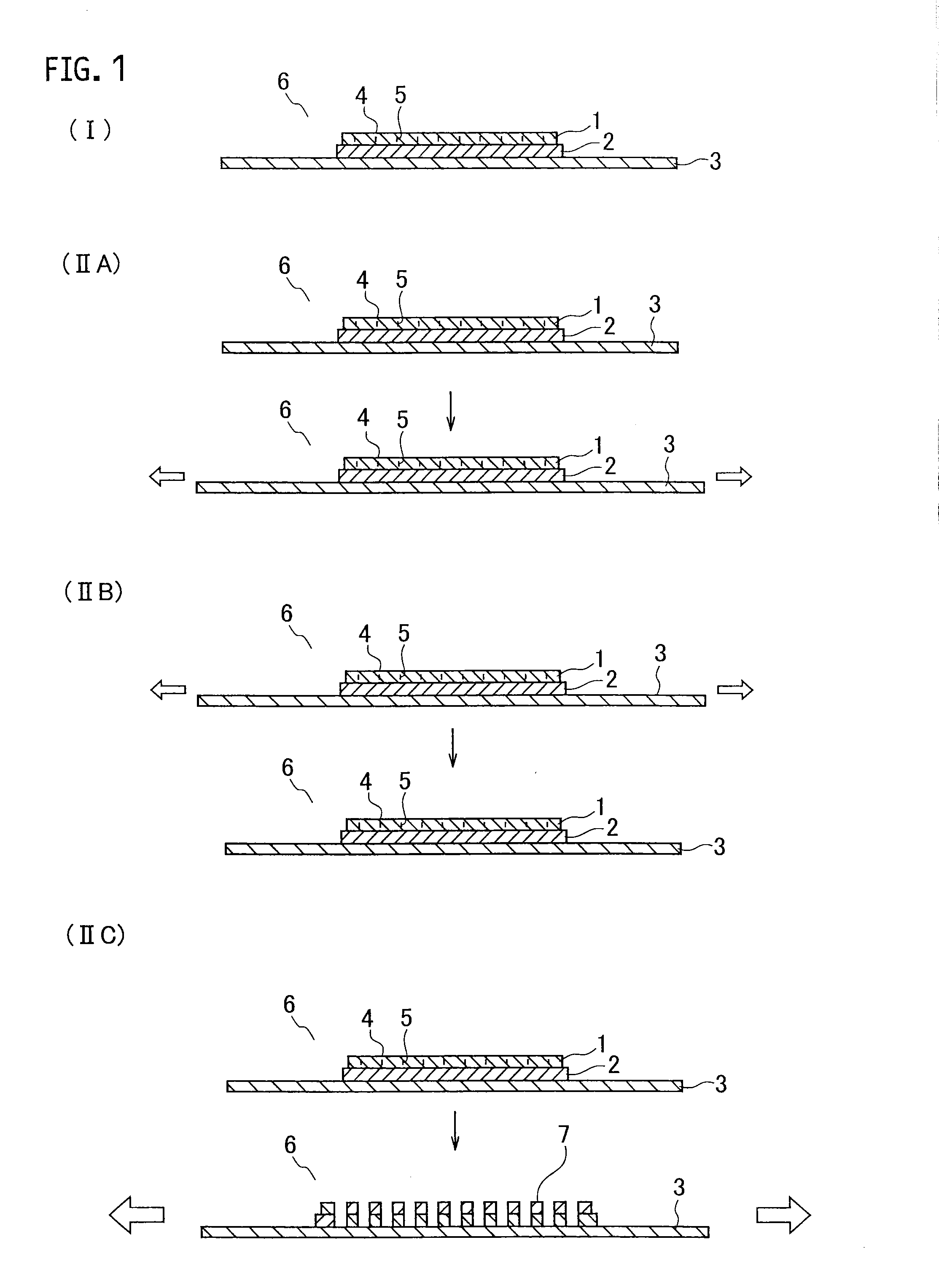
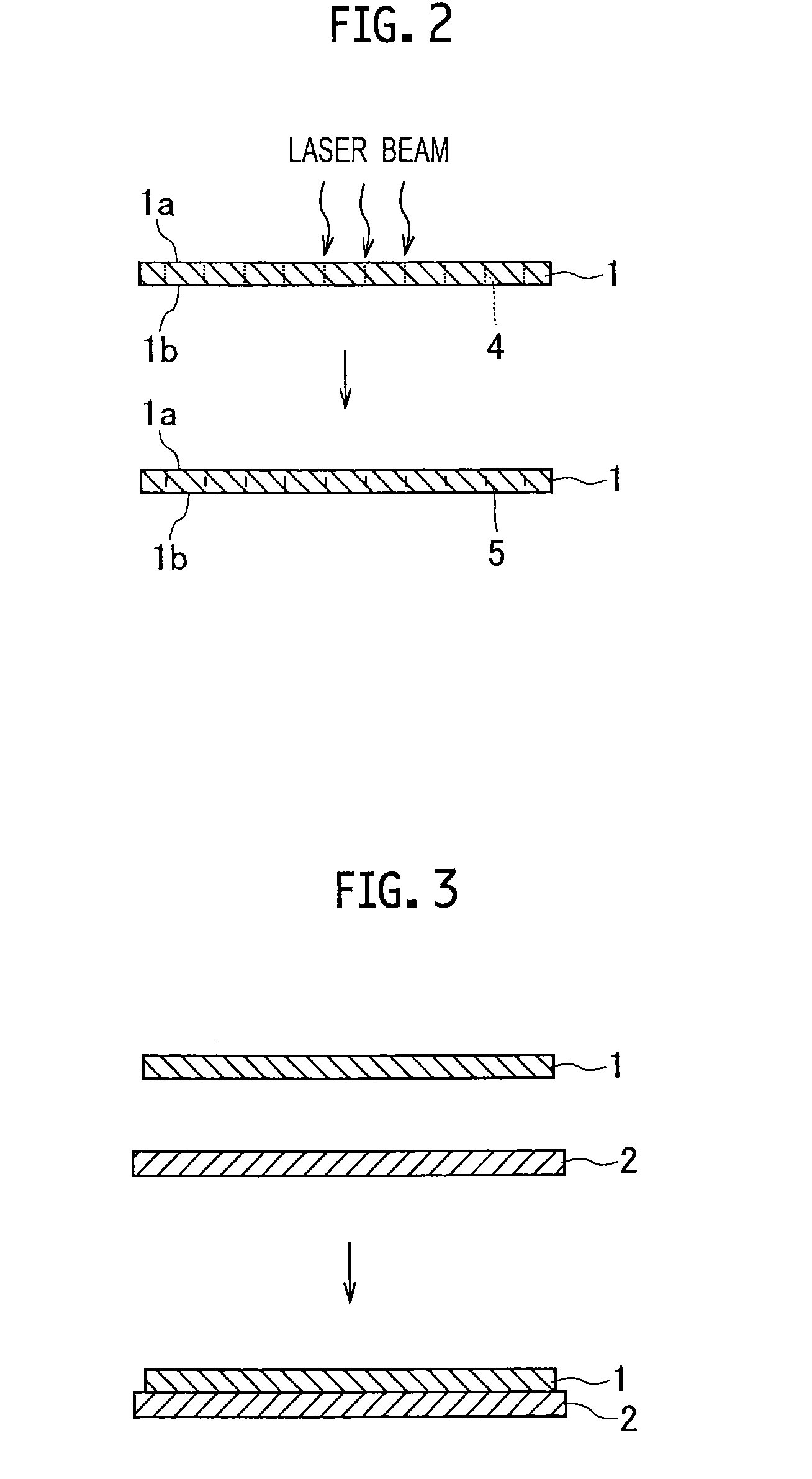
[0041]The first embodiment relates to an expansion method for cutting a semiconductor wafer and a die bonding film along intended cutting lines to divide the wafer into chips, and expanding the spaces between the chips.

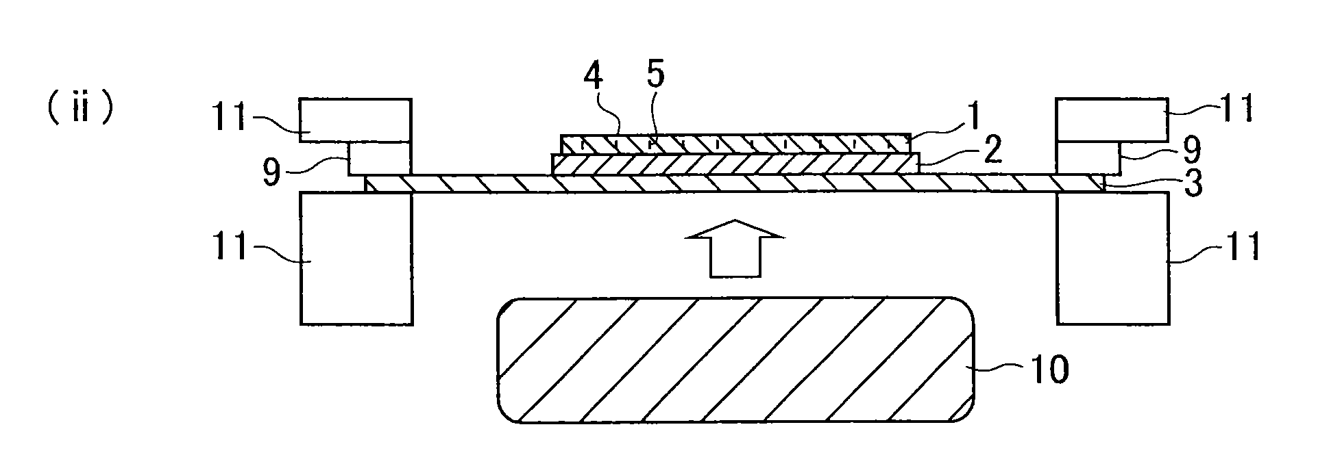
[0042]When cutting a semiconductor wafer and a die bonding film, the expansion step is generally performed at low temperature from the viewpoint of improving the fracture properties of the die bonding film. However, even when the expansion step is performed at low temperature, the semiconductor wafer and the die bonding film can sometimes not be cut. FIG. 18 is a schematic diagram illustrating one example of a conventional expansion method, and shows an example in which a semiconductor wafer 1 and a die bonding film 2 are not cut. In FIG. 18, a dicing tape 3 to which the semiconductor wafer 1 and the die bonding film 2 have been laminated is expanded by pushing the dicing tape 3 upward under cooling using an expansion stage 10 fitted with a cooling device.

[0043]The in...

second embodiment

[0121]The second embodiment relates to an expansion method comprising: a step (Ia) of preparing a laminate having a semiconductor wafer in which modified sections have been formed along intended cutting lines, a die bonding film, a dicing tape and a frame; a step (Ib) of supplying the laminate to the top of a height-adjustable expansion stage of an expansion apparatus comprising the expansion stage and a fastening member capable of fastening the frame; a step (Ic) of fastening the frame using the fastening member; a step (IIa) of raising the expansion stage and expanding the dicing tape with the laminate in a cooled state; a step (IIb) of lowering the raised expansion stage and loosening the expanded dicing tape; and a step (IIc) of raising the expansion stage and expanding the dicing tape with the laminate in a cooled state, dividing the semiconductor wafer and the die bonding film into chips along the intended cutting lines, and widening the spaces between the chips.

[0122]FIG. 6A ...

third embodiment

[0139]The third embodiment relates to an expansion method comprising: a step (Ia′) of preparing a laminate having a semiconductor wafer in which modified sections have been formed along intended cutting lines, a die bonding film, a dicing tape and a frame; a step (Ib′) of supplying the laminate to the top of a height-adjustable expansion ring of an expansion apparatus comprising the expansion ring and a fastening member capable of fastening the frame; a step (Ic′) of fastening the frame using the fastening member; a step (IIa′) of raising the expansion ring and expanding the dicing tape with the laminate in a cooled state; a step (IIb′) of lowering the raised expansion ring and loosening the expanded dicing tape; and a step (IIc′) of raising the expansion ring and expanding the dicing tape with the laminate in a cooled state, dividing the semiconductor wafer and the die bonding film into chips along the intended cutting lines, and widening the spaces between the chips.

[0140]FIG. 7A ...


PUM


Abstract

An embodiment of the present invention relates to an expansion method comprising: a step (I) of preparing a laminate having a semiconductor wafer in which modified sections have been formed along intended cutting lines, a die bonding film and a dicing tape, a step (IIA) of expanding the dicing tape with the laminate in a cooled state, a step (IIB) of loosening the expanded dicing tape, and a step (IIC) of expanding the dicing tape with the laminate in a cooled state, dividing the semiconductor wafer and the die bonding film into chips along the intended cutting lines, and widening the spaces between the chips.

Description

TECHNICAL FIELD[0001]Embodiments of the present invention relate to an expansion method, a method for manufacturing a semiconductor device, and a semiconductor device.BACKGROUND ART[0002]In recent years, remarkable progress has been made in terms of reducing the thickness and size of semiconductor chips. In particular, the semiconductor chips installed in IC cards such as memory cards and smart cards require a chip having a thickness of not more than 75 μm and a size of not more than 10 mm×10 mm. It is thought that as the demand for IC cards increases in the future, the requirement for small, thin chips will continue to grow.[0003]Semiconductor chips are usually obtained by processing a semiconductor wafer to a prescribed thickness in a back grinding step or etching step or the like, and subsequently dividing the semiconductor wafer into individual chips in a dicing step. In the dicing step, a blade cutting method in which the semiconductor wafer is cut with a dicing blade is genera...

Claims


Application Information

Patent Timeline
IPC IPC(8): H01L21/683H01L23/00H01L21/78
CPCH01L21/6836H01L21/78H01L2221/68336H01L24/29H01L24/27H01L21/68H01L2221/68327H01L2221/68377H01L2221/68381H01L24/32H01L24/81H01L2224/32225H01L2224/32245H01L2224/48225H01L2224/48245H01L2224/83191H01L2224/83862H01L2224/94H01L2224/2919H01L2224/73265H01L2924/181H01L2224/32145H01L2224/27H01L2924/00014H01L2924/0665H01L2924/00012H01L21/76
Inventor IWANAGA, YUKIHIROSUZUMURA, KOUJISAKUTA, TATSUYA
Owner RESONAC CORP
Why Eureka
Try Eureka