Display device, and data processing method in display device

a display device and data processing technology, applied in static indicating devices, instruments, electroluminescent light sources, etc., can solve the problems of deterioration of light emission luminance from an initial state, difficult to achieve large size and high definition, etc., to reduce the amount of current data, reduce the amount of high frequency component data and an amount of low frequency component data

Active Publication Date: 2015-12-10
SHARP KK
View PDF9 Cites 36 Cited by
  • Summary
  • Abstract
  • Description
  • Claims
  • Application Information

AI Technical Summary

Benefits of technology

[0080]According to the first aspect of the present invention, in the display device (typically an organic EL display device) employing the electric optical element in which a luminance is controlled by a current as the display element, the following processing is performed on the current data as the compensating data, which is acquired for suppressing “occurrence of burning and variations in luminance” caused by “variations in characteristic of the drive transistor or time degradation of the electric optical element”. First, the current data is divided into the high frequency component data and the low frequency component data. The high frequency component data and the low frequency component data are then compressed by respectively different techniques. Here, for the drive transistor, a transistor with a channel layer formed of an oxide semiconductor (oxide transistor) is employed. According to the present invention, taken into consideration of small variations in characteristic of the oxide transistor, it is possible to reduce an amount of the high frequency component data and an amount of the low frequency component data. With this configuration, it is possible to perform compression processing in consideration of the characteristic of the oxide semiconductor at the time of saving the current data as the compensating data into the storage portion. This allows effective reduction in the amount of the current data to be saved, without causing display failure at the time of displaying an image based on data after decoding. Hence, it is possible to effectively reduce the capacity of the storage portion (

Problems solved by technology

As for an organic EL display device employing the passive matrix technique (hereinafter referred to as “passive matrix type organic EL display device”), its structure is simple, but a large size and high d

Method used


Image

  • Display device, and data processing method in display device
  • Display device, and data processing method in display device
  • Display device, and data processing method in display device

Examples


first embodiment

1. First Embodiment

1.1 Whole Configuration

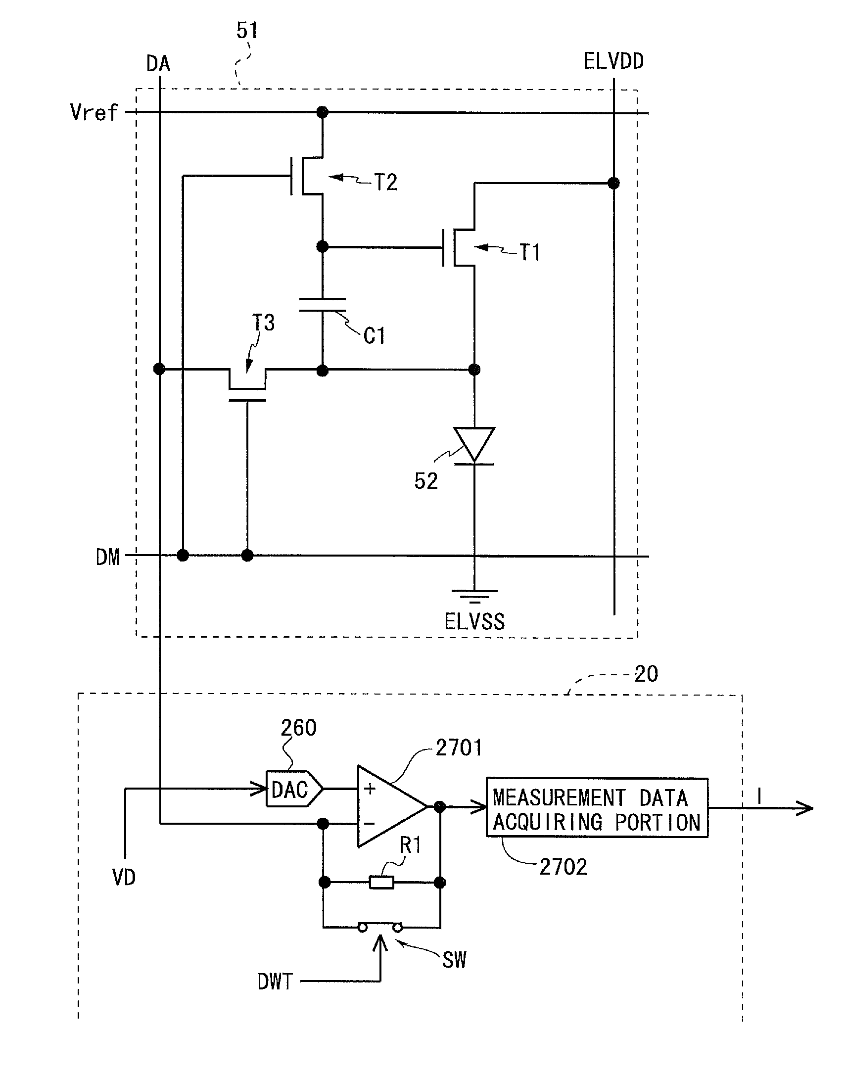
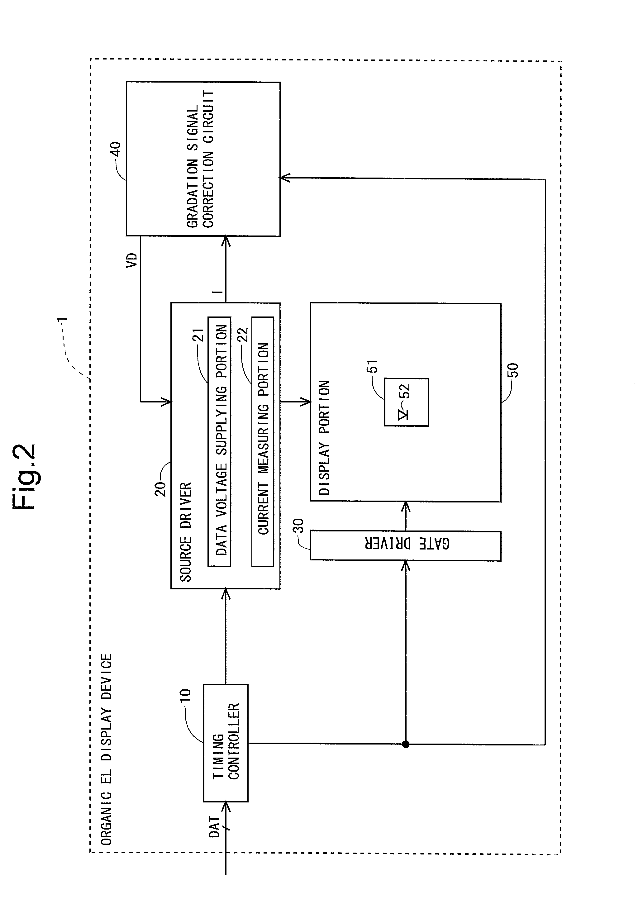
[0133]FIG. 2 is a block diagram showing a whole configuration of an active matrix type organic EL display device 1 according to a first embodiment of the present invention. This organic EL display device 1 includes a timing controller 10, a source driver 20, a gate driver 30, a gradation signal correction circuit 40, and a display portion 50. The source driver 20 includes a data voltage supplying portion 21 and a current measuring portion 22. It should be noted that either the source driver 20 or the gate driver 30, or both of them, may be configured to be integrally formed with the display portion 50. The display portion 50 is formed with a plurality of pixel circuits 51 including an OLED 52 as an electric optical element. A detailed configuration of the pixel circuit 51 will be described later. It should be noted that FIG. 2 shows only one pixel circuit 51.

[0134]FIG. 3 is a block diagram for describing a configuration of the display portio...

second embodiment

2. Second Embodiment

[0221]Hereinafter, only a matter different from the first embodiment will be described, and a description of a similar matter to the first embodiment will be omitted. It should be noted that, in the present embodiment and a third embodiment described later, with regard to a display device having 1920×1080 pixels, the storage portion for high frequency component data after compression out of the prepared storage portion (memory) 480 is assumed to be 2M bits, for the sake of simplifying the description. In addition, each pixel data is assumed to be 6 bits. In this case, a data amount D1 of the pixel current data I before compression is as follows:

D1=6×1,920×1,080=12,441,600 bits (about 11.87 megabits)

[0222]Therefore, a compression ratio of about 17% has to be realized.

[0223]When the compression processing is performed while a compression parameter is controlled one row by one row, an average data amount D2 per row with respect to the pixel current data I after comp...

third embodiment

3. Third Embodiment

3.1 Compression Technique

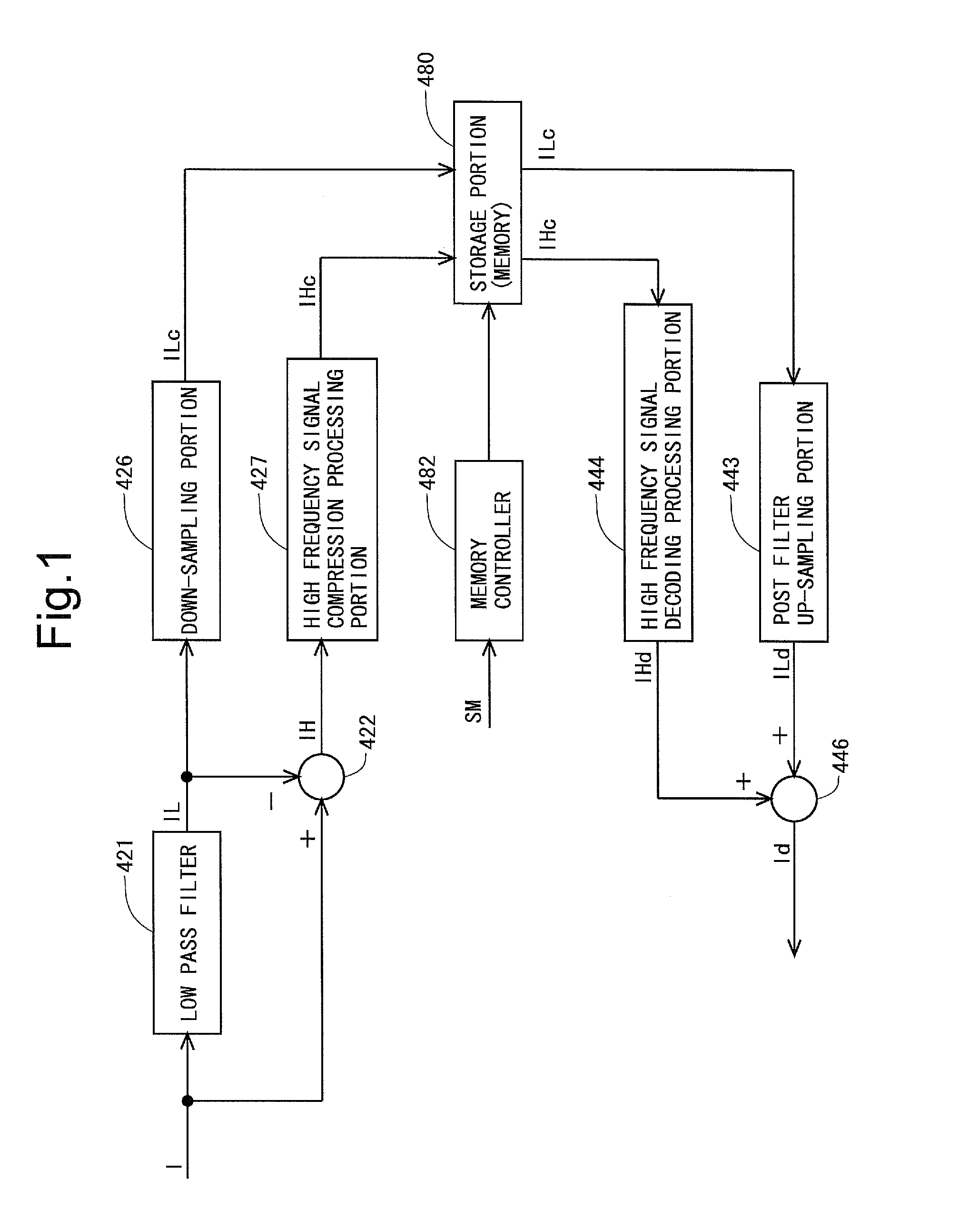
[0235]In the present embodiment, a compression method for the high frequency component data IH is different from that in the first embodiment. Therefore, in the following, a description will be given of the compression method for the high frequency component data IH in the present embodiment (hereinafter referred to as “re-quantization technique”). In the re-quantization technique, multiplication of data (high frequency component data IH) and a predetermined coefficient is performed before re-quantization, and a value of the coefficient for the multiplication is set to the compression parameter P. As the value of the compression parameter P decreases, a value of data obtained by the multiplication approaches “0”, and a length of Huffman coding is shorter. Accordingly, the compression ratio increases, and the amount of the data after compression (compressed high frequency component data IHc) decreases. Hereinafter, this will be described in...


PUM


Abstract

An embodiment of the present invention is directed to reducing a memory capacity required for saving compensating data (data used for compensating variations and the like in characteristic of a drive transistor) compared to conventional examples, in a display device. An organic EL display device using an oxide TFT for a drive transistor is provided with: a low pass filter for extracting low frequency component data from pixel current data as data of a drive current of the drive transistor; a first computing portion for obtaining high frequency component data by obtaining a difference between the pixel current data and the low frequency component data; a down-sampling portion for extracting data from the low frequency component data at predetermined sampling intervals; and a high frequency signal compression processing portion for extracting only high amplitude data out of the high frequency component data.

Description

TECHNICAL FIELD[0001]The present invention relates to a display device, and more specifically relates to a display device using an electric optical element such as an organic light emitting diode (OLED) as a display element, and a data processing method in the display device.BACKGROUND ART[0002]As a display element provided in a display device, there have conventionally been an electric optical element in which a luminance is controlled by an applied voltage and an electric optical element in which a luminance is controlled by a flowing current. Typical examples of the electric optical element in which a luminance is controlled by an applied voltage include a liquid crystal display element. Typical examples of the electric optical element in which a luminance is controlled by a flowing current include an OLED. The OLED is also called an organic electro luminescence (EL) element. An organic EL display device that uses the OLED being a spontaneous light-emitting electric optical eleme...

Claims


Application Information

Patent Timeline
IPC IPC(8): G09G3/14G09G3/20G09G3/32H05B44/00
CPCG09G3/14G09G3/3258G09G3/3233G09G3/3283G09G2320/0633G09G2300/08G09G2320/0271G09G2320/046G09G3/2011G09G3/3225G09G2300/0842G09G2320/0233G09G2320/045G09G2340/02H10K50/00
Inventor YAMANAKA, SHIGETSUGUNAKAGAWA, SHINJIFURUKAWA, HIROYUKIOHTA, YOSHIFUMI
Owner SHARP KK
Why Eureka
Try Eureka