Method and system for an optoelectronic built-in self-test system for silicon photonics optical transceivers

a self-testing, optoelectronic technology, applied in electromagnetic transceivers, digital transmission, transmission monitoring, etc., can solve the problems of cable bulk penalties, large power requirements, and complex structure, and achieve only modest improvements in reach and limited scalability

Active Publication Date: 2015-12-31
CISCO TECH INC
View PDF8 Cites 35 Cited by
  • Summary
  • Abstract
  • Description
  • Claims
  • Application Information

AI Technical Summary

Benefits of technology

[0004]Further limitations and disadvantages of conventional and traditional approaches will become apparent to one of skill in the art, through comparison of such systems with the present disclosure as set forth in the remainder of the present application with reference to the drawings.

Problems solved by technology

They can be mitigated to some extent with equalization, coding, and shielding, but these techniques require considerable power, complexity, and cable bulk penalties while offering only modest improvements in reach and very limited scalability.

Method used


Image

  • Method and system for an optoelectronic built-in self-test system for silicon photonics optical transceivers
  • Method and system for an optoelectronic built-in self-test system for silicon photonics optical transceivers
  • Method and system for an optoelectronic built-in self-test system for silicon photonics optical transceivers

Examples


Embodiment Construction

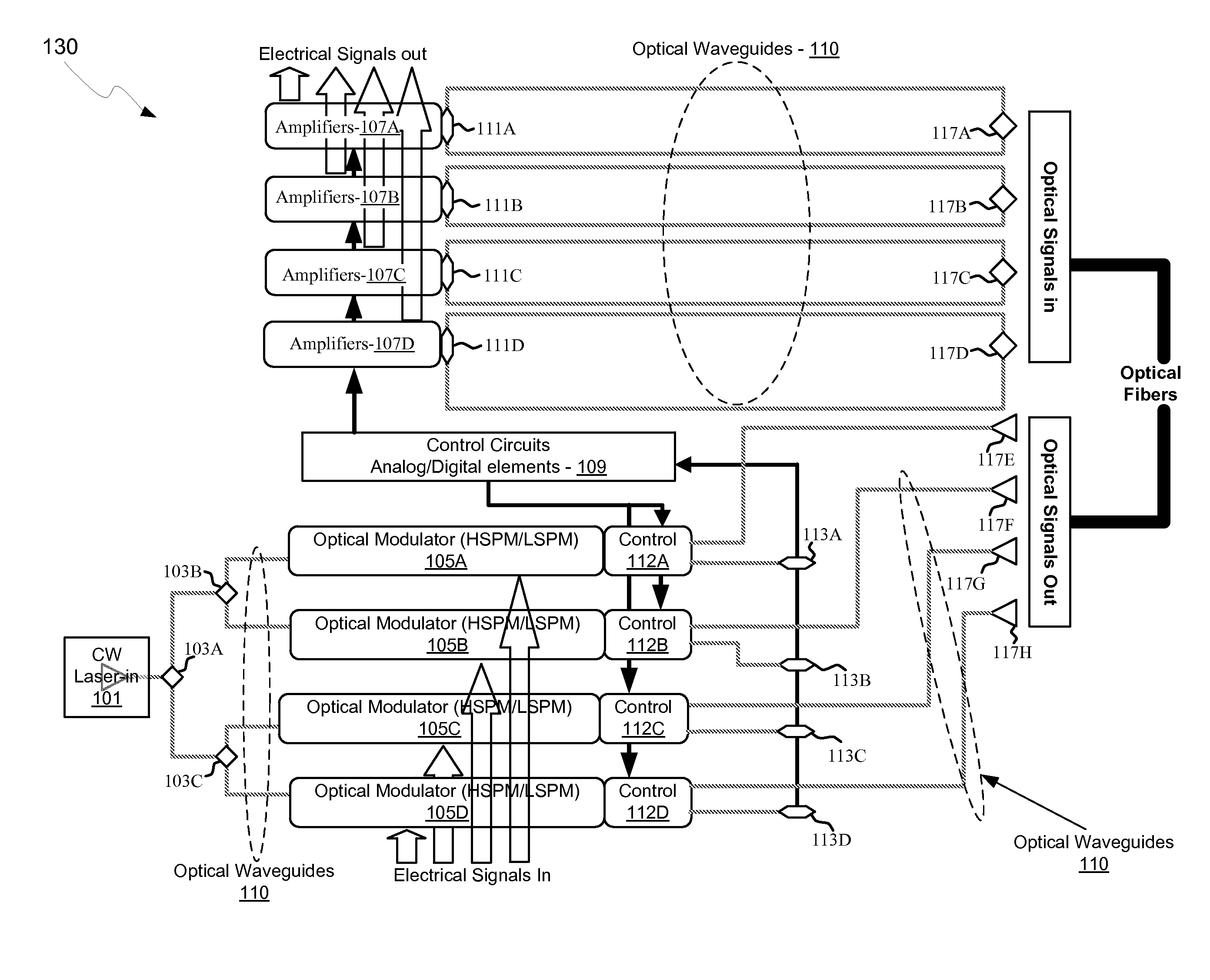
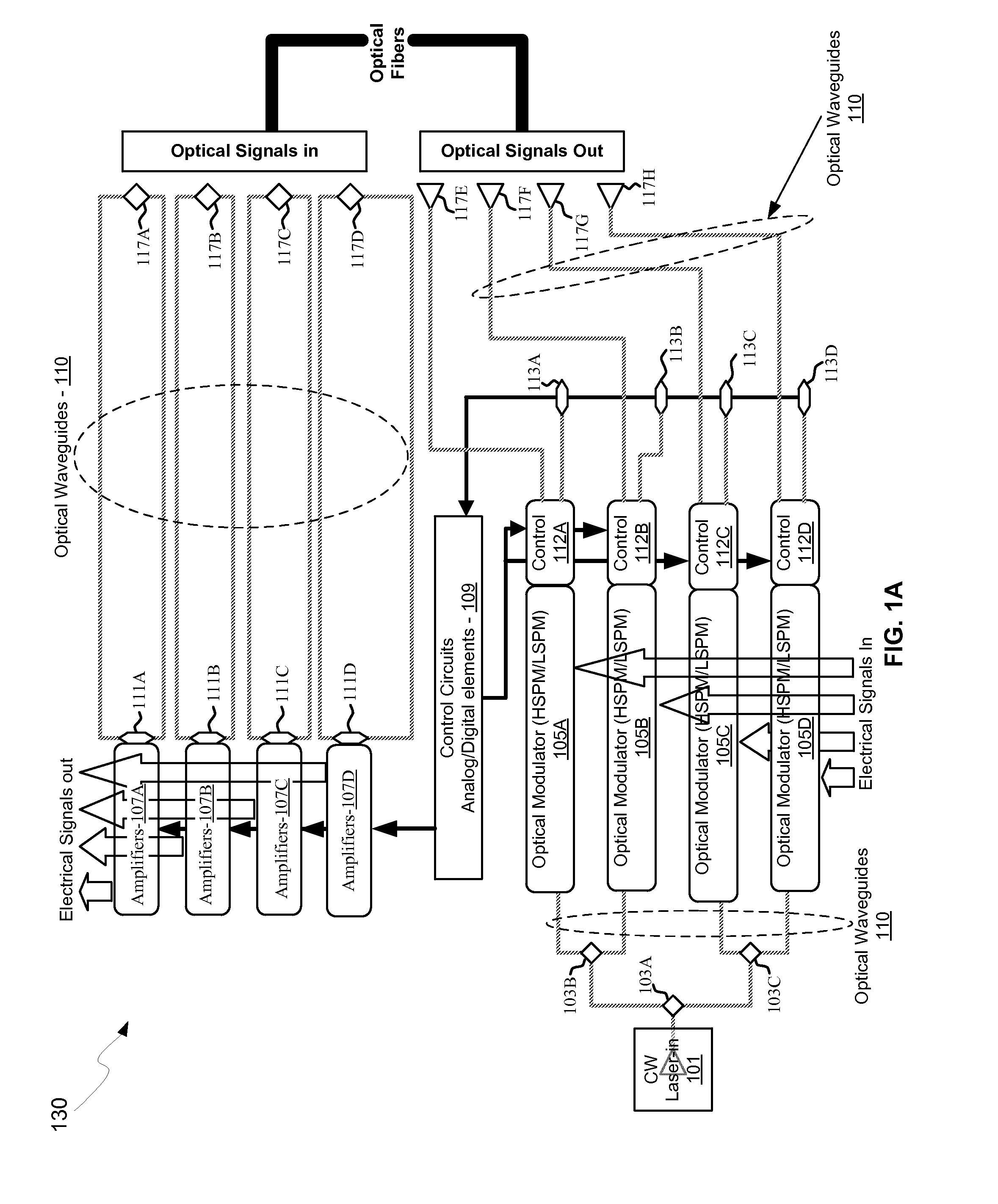
[0014]Certain aspects of the disclosure may be found in a method and system for an optoelectronic built-in self-test system for silicon photonics optical transceivers. Exemplary aspects of the disclosure may comprise, in an optoelectronic transceiver having a transmit (Tx) path and a receive (Rx) path, where the Rx path comprises a main Rx path and a built-in self-test loopback path: generating a pseudo-random bit sequence (PRBS) signal, generating an optical signal in the Tx path by applying the PRBS signal to an optical modulator, communicating the optical signal to the built-in self-test loopback path, converting the optical signal to an electrical signal in the Rx path utilizing a loopback photodetector in the built-in self-test loopback path, where the loopback photodetector is a replica of a photodetector in the main Rx path, and assessing the performance of the Tx and Rx paths by extracting a PRBS signal from the electrical signal. The optoelectronic transceiver may be in a s...


PUM


Abstract

Methods and systems for an optoelectronic built-in self-test (BIST) system for silicon photonics optical transceivers are disclosed and may include, in an optoelectronic transceiver having a transmit (Tx) path and a receive (Rx) path, where the Rx path includes a main Rx path and a BIST loopback path: generating a pseudo-random bit sequence (PRBS) signal, generating an optical signal in the Tx path by applying the PRBS signal to a modulator, communicating the optical signal to the BIST loopback path and converting to an electrical signal utilizing a photodetector, the photodetector being a replica of a photodetector in the main Rx path, and assessing the performance of the Tx and Rx paths by extracting a PRBS signal from the electrical signal. The transceiver may be a single complementary-metal oxide semiconductor (CMOS) die or in two CMOS die, where a first comprises electronic devices and a second comprises optical devices.

Description

CROSS-REFERENCE TO RELATED APPLICATIONS / INCORPORATION BY REFERENCE[0001]This application claims priority to and the benefit of U.S. Provisional Application 61 / 998,396 filed on Jun. 26, 2014, which is hereby incorporated herein by reference in its entirety.FIELD[0002]Certain embodiments of the disclosure relate to semiconductor photonics. More specifically, certain embodiments of the disclosure relate to a method and system for an optoelectronic built-in self-test system for silicon photonics optical transceivers.BACKGROUND[0003]As data networks scale to meet ever-increasing bandwidth requirements, the shortcomings of copper data channels are becoming apparent. Signal attenuation and crosstalk due to radiated electromagnetic energy are the main impediments encountered by designers of such systems. They can be mitigated to some extent with equalization, coding, and shielding, but these techniques require considerable power, complexity, and cable bulk penalties while offering only mode...

Claims


Application Information

Patent Timeline
Patent Type & Authority Applications(United States)
IPC IPC(8): H04B10/077H04L1/24H04B10/40
CPCH04B10/40H04L1/244H04B10/801H04B10/0779H04L1/243
Inventor GLOECKNER, STEFFENSAHNI, SUBALBALARDETA, JOSEPHPANG, SIMONDENTON, SCOTT
Owner CISCO TECH INC
Why Eureka
Try Eureka