
Package structure and fabrication method thereof

Inactive Publication Date: 2016-01-07
SILICONWARE PRECISION IND CO LTD
View PDF7 Cites 8 Cited by
  • Summary
  • Abstract
  • Description
  • Claims
  • Application Information

AI Technical Summary

Benefits of technology

The present invention provides a positioning unit that helps to create open areas in a resist layer for an electronic element. This positioning unit is easy to detect and align with an aligning device. As a result, each circuit layer can be aligned at the same position, overcoming the conventional drawbacks.

Problems solved by technology

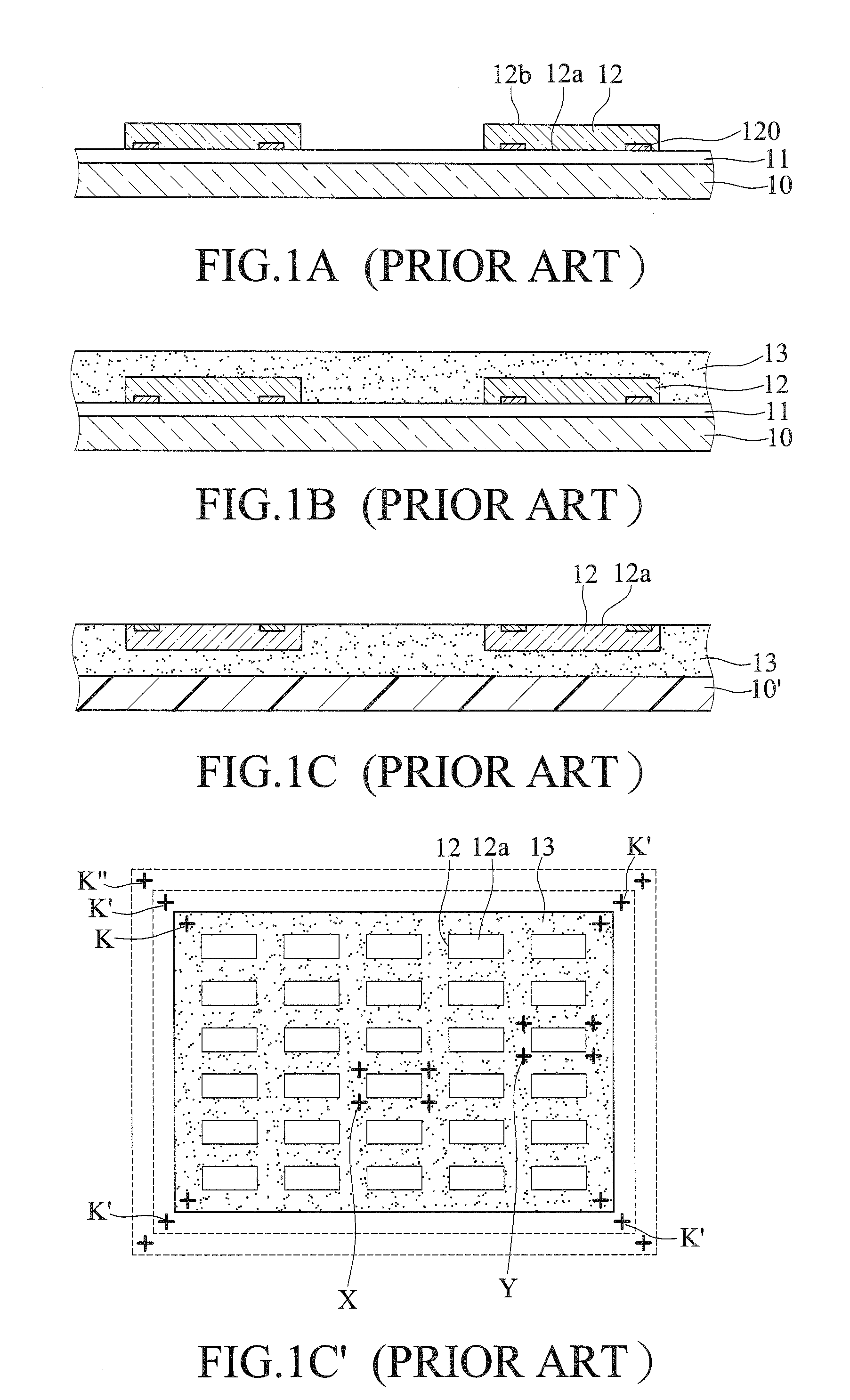
However, in the above-described fabrication method of the semiconductor package 1, the positioning marks K, K′, K″ are difficult to be read by an exposure device due to an interference of the circuit portions 141 made of a metal material.
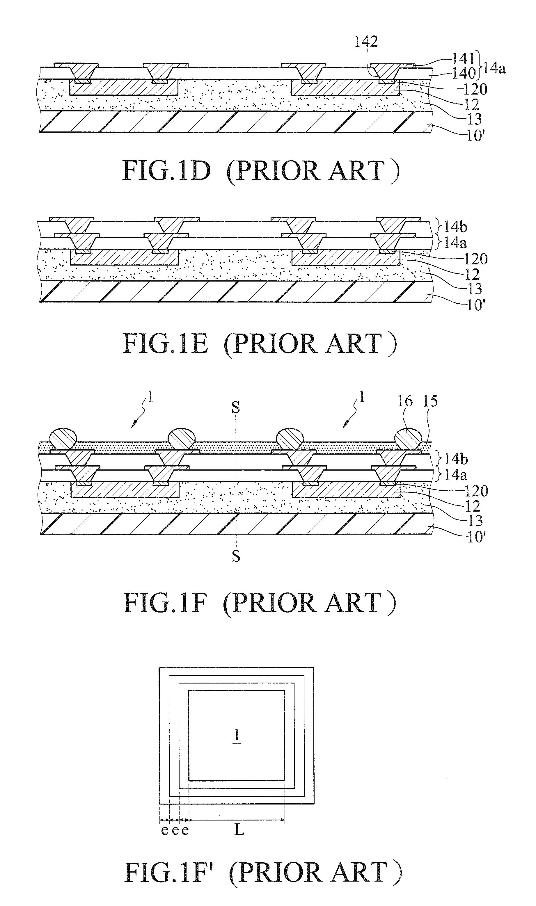
The exposure alignment process of each stack layer incurs an accumulation of the alignment error of the semiconductor package 1.

Method used


Image

  • Package structure and fabrication method thereof
  • Package structure and fabrication method thereof
  • Package structure and fabrication method thereof

Examples


first embodiment

[0042]FIGS. 2A through 2D are schematic cross-sectional views showing a method for fabricating a package structure 2 according to the present invention.

[0043]Referring to FIG. 2A, a package 20 is provided. The package 20 has a base portion 23, a plurality of electronic elements 22 embedded in the base portion 23, and a plurality of positioning units 21 formed on the base portion 23 around peripheries of the electronic elements 22. The base portion 23 has opposite first and second surfaces 23a, 23b, and the positioning units 21 protrude from the first surface 23a of the base portion 23.

[0044]In the present embodiment, the processes of the base portion 23 and the electronic elements 22 are similar to the processes of FIGS. 1A through 1C (the carrier is omitted in FIG. 2A). Then, referring to FIG. 2A′, four blocks are formed on corners of the first surface 23a of the base portion 23 to serve as the positioning units 21. As such, the package 20 is obtained. In particular, at least one p...

second embodiment

[0062]FIGS. 3A through 3E are schematic cross-sectional views showing a method for fabricating a package structure 3 according to the present invention. In the present embodiment, each of the positioning units 31 has a positioning base 311 and at least a positioning portion 310 formed on the positioning base 311. The positioning units 31 and at least an electronic element 22 are embedded in a base portion 23 through a same process.

[0063]Referring to FIG. 3A, at least a positioning unit 31 and the electronic element 22 are disposed on a bonding layer 400 of a carrier 40.

[0064]In the present embodiment, the positioning base 311 is a dummy die having no electrical function or a semiconductor die having a certain function. The positioning base 311 has a positioning pad serving as the positioning portion 310. The positioning portion 310 is embedded in the bonding layer 400.

[0065]The positioning portion 310 is made of electroplated aluminum, electroplated copper, a coated and etched metal...

fourth embodiment

[0086]FIG. 7 is a schematic cross-sectional view showing a method for fabricating a package structure 7 according to the present invention. In the present embodiment, different types of positioning units are provided.

[0087]Referring to FIG. 7, the package structure 7 has a positioning unit 21 protruding from the first surface 23a of the base portion 23 and a positioning unit 21″ recessed from the first surface 23a of the base portion 23. In other embodiments, the positioning units of FIGS. 2C-1 through 2C-3 and FIGS. 5-1 through 5-6 can be combined to provide various configurations.

[0088]The present invention provides a positioning structure, which has: a base portion 23 having opposite first and second surfaces 23a, 23b; and at least a positioning unit 21, 21′, 21″, 21b, 31, 31′, 31″, 31a, 51, 51′ in contact with the base portion 23. The present invention further provides a package structure 2, 2′, 2b, 3, 4, 7, which has: the above-described positioning structure; and at least an e...


PUM


Abstract

A method for fabricating a package structure is provided, which includes the steps of: providing a base portion having at least an electronic element embedded therein and at least a positioning unit formed around a periphery of the electronic element, wherein the positioning unit protrudes from or is flush with a surface of the base portion; and forming at least a circuit layer on the surface of the base portion and the electronic element. The circuit layer is aligned and connected to the electronic element through the positioning unit.

Description

BACKGROUND OF THE INVENTION[0001]1. Field of the Invention[0002]The present invention relates to package structures and fabrication methods thereof, and more particularly, to a package structure having a positioning structure and a fabrication method thereof.[0003]2. Description of Related Art[0004]Along with the rapid development of electronic industries, electronic products are developed toward the trend of multi-function and high performance. Accordingly, wafer level packaging (WLP) technologies have been developed to meet the miniaturization requirement of semiconductor packages.[0005]FIGS. 1A through 1F are schematic cross-sectional views showing a method for fabricating a wafer level fan-out semiconductor package 1 according to the prior art.[0006]Referring to FIG. 1A, a thermal release tape 11 is formed on a carrier 10, and then a plurality of semiconductor elements 12 are disposed on the thermal release tape 11. Each of the semiconductor elements 12 has an active surface 12a...

Claims


Application Information

Patent Timeline
IPC IPC(8): H01L23/544H01L21/52
CPCH01L21/52H01L23/544H01L21/561H01L21/568H01L23/3128H01L24/19H01L24/96H01L24/97H01L2223/5442H01L2223/54426H01L2223/54486H01L2224/04105H01L2224/12105H01L21/682H01L23/15H01L23/3121H01L23/3135H01L2223/54453H01L2224/02331H01L2224/02372H01L2224/0401H01L2224/05022H01L2224/05025H01L2224/05073H01L2224/05563H01L2224/05567H01L2224/05569H01L2224/05573
Inventor TAI, RUI-FENGHUANG, HSIAO-CHUNLU, CHUN-HUNGHSU, HSI-CHANGCHEN, SHIH-CHING
Owner SILICONWARE PRECISION IND CO LTD
Learn More