
Memory controller, nonvolatile storage module, access module and nonvolatile storage system

Active Publication Date: 2011-08-11
SK HYNIX INC
View PDF5 Cites 10 Cited by
  • Summary
  • Abstract
  • Description
  • Claims
  • Application Information

AI Technical Summary

Benefits of technology

[0029]According to the present invention, based on determination of a writing destination area by selection of the free area by the address management unit, that is, wear leveling by the alternate processing, the recording state judgement unit performs the swap necessity judgement according to the recording state and the reading and writing control unit performs determination of the swap target area and swap according to the swap necessity judgement. Thus, the localization of alternate area as the above-mentioned problem in Patent document 1 can be solved and the lifetime of the nonvolatile storage module can be extended. Furthermore, according to the present invention, since new data is written to the free physical block, the power disconnection problem as the second problem in Patent document 2 can be solved.
[0030]Since the recording state judgement unit detects the alternate area localization, swap can be performed when the alternate area is localized. Furthermore, the alternate area localization can be easily detected based on the number of times of rewriting of the physical block. In addition, swap can be effectively performed by determining the swap target based on the number of times of rewriting or a state whether or not the block is a free block in addition to the number.

Problems solved by technology

Although the semiconductor memory card is much more expensive than an optical disc or a tape media, due to small size, light weight, seismicity and convenience in handling, it is in great demand as a recording medium for portable devices such as digital still cameras and mobile phones.
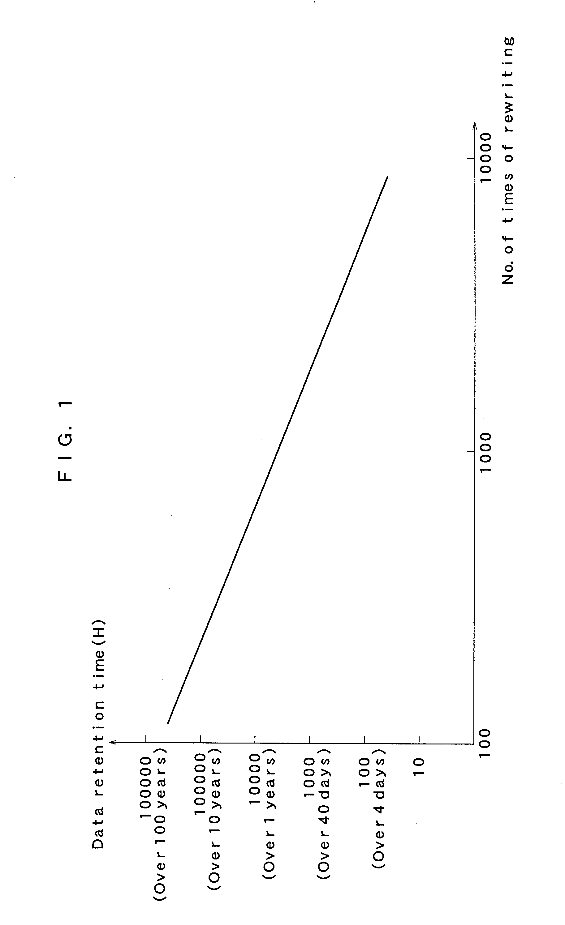
In the multi-level NAND flash memory, it is difficult to ensure reliability of the memory cell and therefore, the number of times of rewriting is small.

Method used


Image

  • Memory controller, nonvolatile storage module, access module and nonvolatile storage system
  • Memory controller, nonvolatile storage module, access module and nonvolatile storage system
  • Memory controller, nonvolatile storage module, access module and nonvolatile storage system

Examples


first embodiment

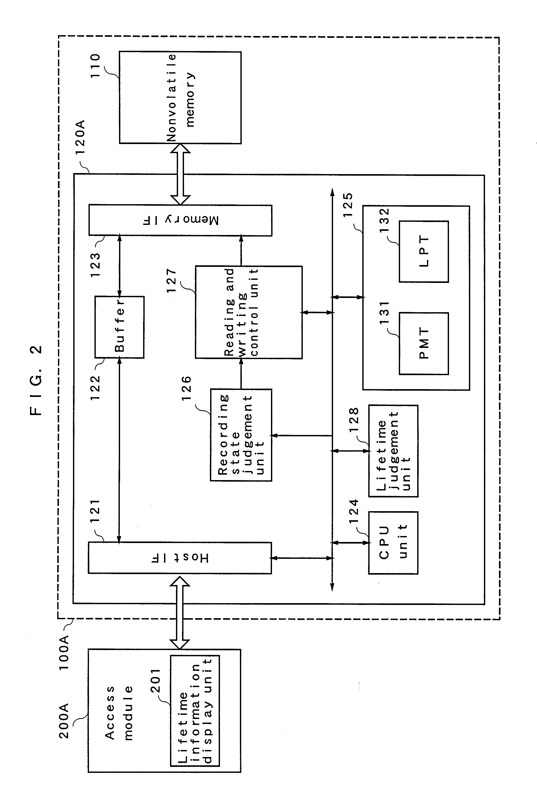
[0086]FIG. 2 is a block diagram showing a nonvolatile storage system in accordance with a first embodiment of the present invention. In FIG. 2, the nonvolatile storage system includes a nonvolatile storage module 100A and an access module 200A. The access module 200A includes a lifetime information display unit 201. The nonvolatile storage module 100A includes a nonvolatile memory 110 and memory controller 120A. The memory controller 120A includes a host interface (host IF) 121, a buffer 122, a memory interface (memory IF) 123, a CPU unit 124, an address management unit 125, a recording state judgement unit 126, a reading and writing control unit 127 and a lifetime judgement unit 128.

[0087]The nonvolatile memory 110 is a flash memory and has P physical blocks. The physical block is an erasing unit and all of the P physical blocks are used for data recording. The physical block is a writing unit and consists of a plurality of pages. It is assumed that a logical space which can be use...

second embodiment

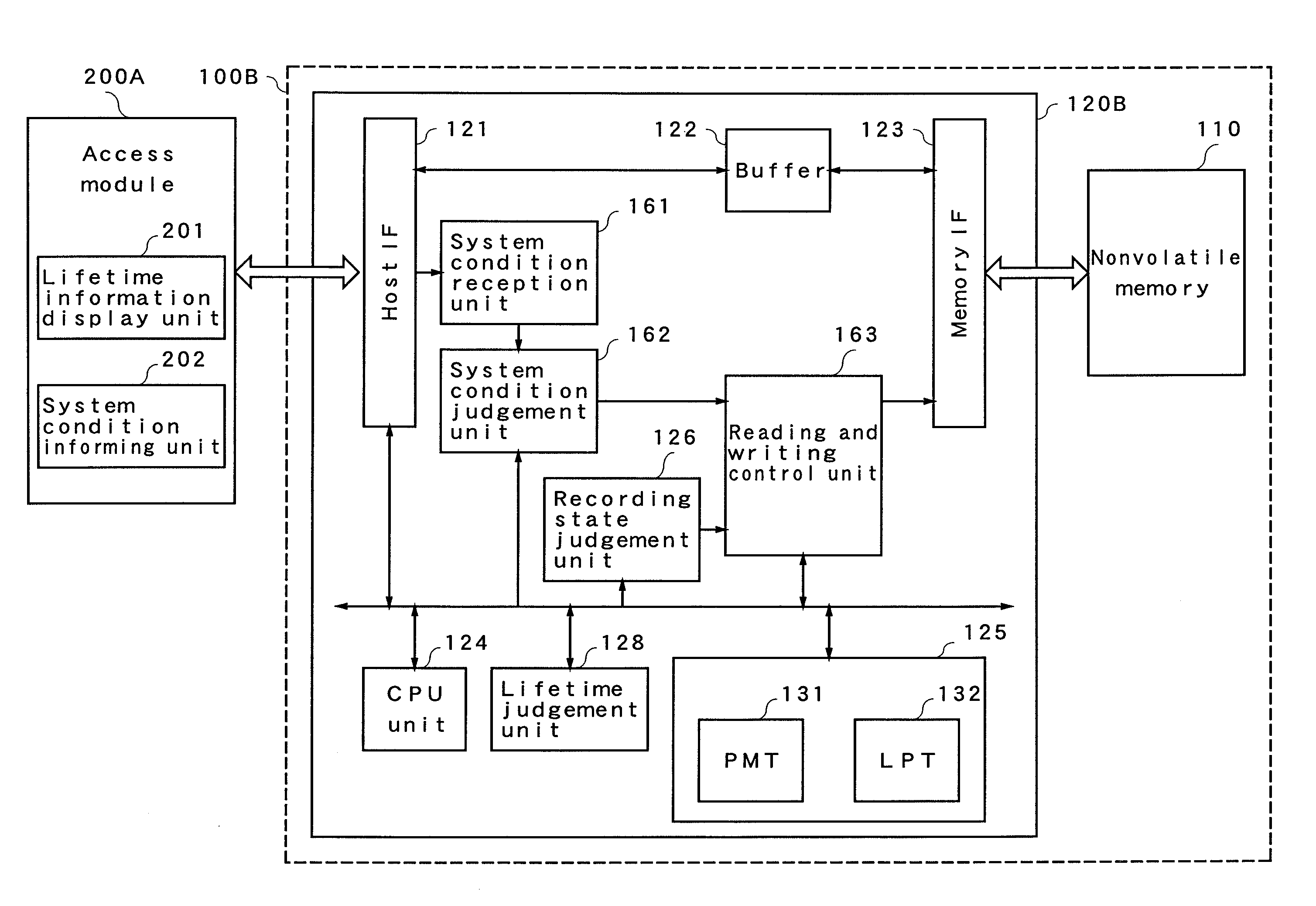
[0159]FIG. 15 is a block diagram showing a nonvolatile storage system in accordance with a second embodiment of the present invention. In FIG. 15, the nonvolatile storage system includes a nonvolatile storage module 100B and access module 200B. The access module 200B is obtained by adding a system condition informing unit 202 to the access module in the first embodiment. The nonvolatile storage module 100B includes a memory controller 120B and nonvolatile memory 110. The memory controller 120B is obtained by adding a system condition reception unit 161 and system condition judgement unit 162 to the memory controller 120A in the first embodiment. The reading and writing control unit 163 is a modification of the reading and writing control unit 127 in the first embodiment. The other blocks are similar to those in the nonvolatile storage module in the first embodiment in FIG. 1.

[0160]Operation of the nonvolatile storage system thus configured in accordance with the second embodiment of...

third embodiment

[0178]FIG. 21 is a block diagram showing a nonvolatile storage system in accordance with a third embodiment of the present invention. The nonvolatile storage system includes a nonvolatile storage module 100C and an access module 200A. The access module 200A is same as the access module in the first embodiment. The nonvolatile storage module 100C includes a system condition reception unit 171, system condition judgement unit 172 and reading and writing control unit 173, and the other blocks are similar to those in the nonvolatile storage system in the second embodiment shown in FIG. 15.

[0179]Operation of the nonvolatile storage system thus configured in accordance with the third embodiment of the present invention will be described. FIG. 22 is a flow chart showing processing by the nonvolatile storage module 100C in accordance with the third embodiment of the present invention. A basic operation of the nonvolatile storage system is similar to that of the nonvolatile storage system in...


PUM


Abstract

When a write command is issued, new data is written into a free physical block of a nonvolatile memory (110). Here, if data of the same logical block has been written already, the block is erased and a recording state is judged by a recording state judgment unit (126). A physical block is swapped according to the number of write processes performed. Thus, it is possible to effectively perform a swap without increasing the number of write processes in a particular area, thereby increasing the lifetime of a nonvolatile storage module.

Description

TECHNICAL FIELD[0001]The present invention relates to a nonvolatile storage module such as a semiconductor memory card having a nonvolatile memory, a memory controller for controlling the nonvolatile memory, an access module and nonvolatile storage system formed by adding the access module as a structural element to the nonvolatile storage module.BACKGROUND ART[0002]A nonvolatile storage module having a rewritable nonvolatile memory, which is typified by a semiconductor memory card, has been increasingly demanded as a removable storage device. Although the semiconductor memory card is much more expensive than an optical disc or a tape media, due to small size, light weight, seismicity and convenience in handling, it is in great demand as a recording medium for portable devices such as digital still cameras and mobile phones. In recent years, with an increase in capacity of the semiconductor memory card, application of the memory card to an alternative device for a hard disc of a per...

Claims


Application Information

Patent Timeline
IPC IPC(8): G06F12/00
CPCG06F11/1441G06F2212/7211G06F2212/1036G06F12/0246
Inventor NAKANISHI, MASAHIROADACHI, TATSUYA
Owner SK HYNIX INC
Learn More