
Installation for processing a paper web or corrugated cardboard web

a technology of corrugated cardboard and paper web, which is applied in the field of installation for processing corrugated cardboard web, can solve the problems of frequent false alarms, complex and expensive, and inability to detect the position of defects, and achieve the effect of cost-effective and simple, and preventing false alarms

Active Publication Date: 2016-01-14
BHS CORRUGATED MASCHEN & ANLAGENBAU
View PDF6 Cites 5 Cited by
  • Summary
  • Abstract
  • Description
  • Claims
  • Application Information

AI Technical Summary

Benefits of technology

The invention is a device and method for detecting material defects in a printing device. The device is designed to be cost-effective and simple, with the goal of preventing false alarms and ensuring safe and effective detection of material defects. The technical effects of this invention include improved efficiency and accuracy in detecting material defects, as well as reduced likelihood of damage to the printing device caused by material defects.

Problems solved by technology

Profile sensor devices of this type need to be arranged in a horizontal cascade which makes them extremely complex and expensive.
These systems are however unable to detect the position of the defect.
Another problem of these known solutions is that false alarms occur frequently.
Material defects of this type may result in severe damages during subsequent processing of the material web.
The damages may occur on processing devices, on the material web itself or on the surroundings.
In many cases, the material defects cause damages in particular in digital printing devices such as inkjet digital printing devices since these devices usually comprise sensitive fine ceramic components.

Method used


Image

  • Installation for processing a paper web or corrugated cardboard web
  • Installation for processing a paper web or corrugated cardboard web
  • Installation for processing a paper web or corrugated cardboard web

Examples


Embodiment Construction

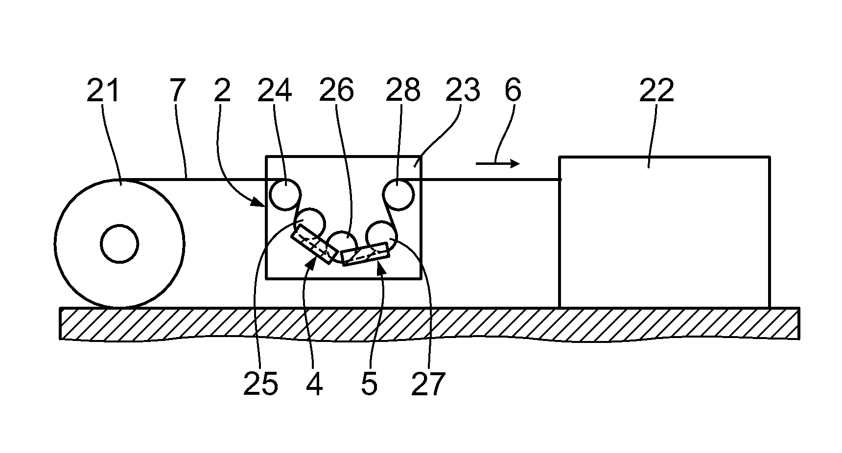
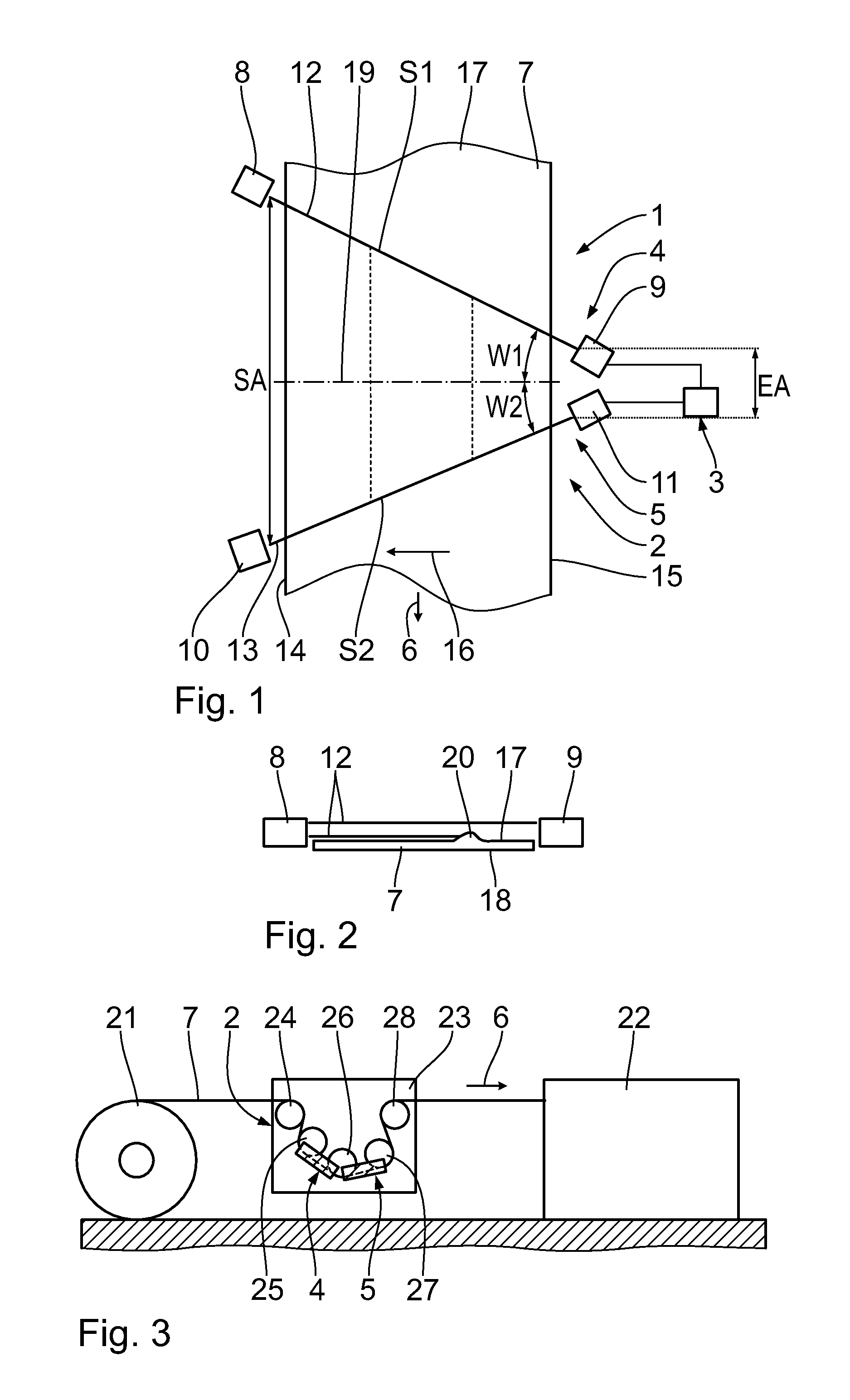
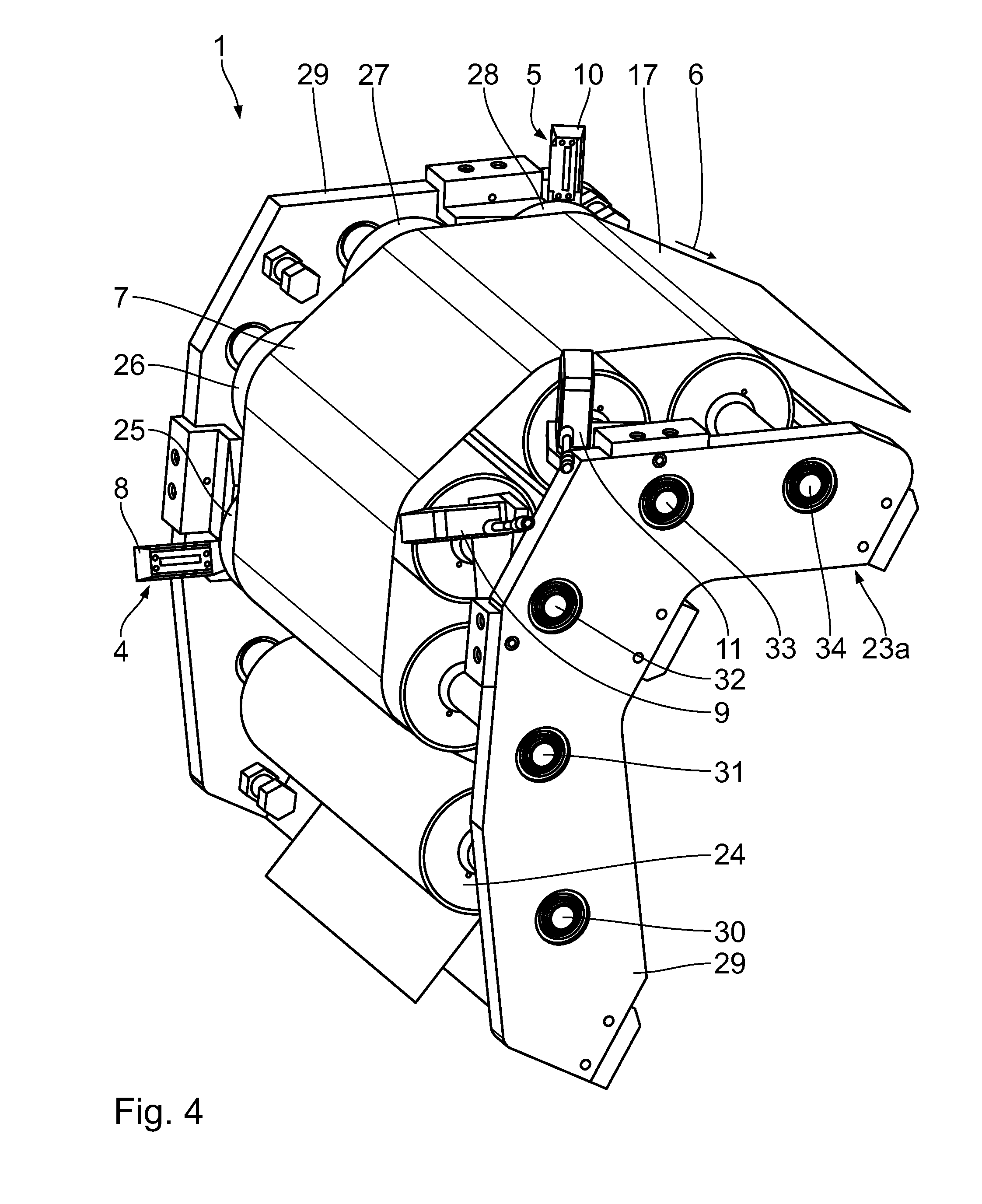
[0047]Referring to FIGS. 1, 2, the following is a description of a simplified material defect detection device 1. The material defect detection device 1 comprises a sensor device 2 and a signal evaluation unit 3 which is in signal communication with the sensor device 2. The sensor device 2 in turn comprises a first sensor unit 4 and a second sensor unit 5 which is preferably identical to the first sensor unit 4. Seen in the feed direction 6 of a material web 7 to be monitored, the second sensor unit 5 is arranged downstream of the first sensor unit 4. The sensor units 4, 5 are arranged next to the material web 7. More precisely, they are in each case arranged on the sides next to the material web 7.

[0048]The first sensor unit 4 has a first emitter 8 and a first receiver 9 assigned to said first emitter 8. The second sensor unit 5 on the other hand has a second emitter 10 and a second receiver 11 assigned to said second emitter 10. The first emitter 8 emits first light sensor beams 1...


PUM


Abstract

An installation for the detection of projecting material defects in a paper web or corrugated cardboard web moved in a feed direction. The device comprises a sensor device comprising a first sensor unit with a first emitter for emitting first sensor beams and a second emitter for emitting second sensor beams and with a second receiver, wherein the first sensor beams run parallel to the material surface to be monitored of the paper web or corrugated cardboard web and travel along a first signal path S1 in-between. The sensor device further has a second sensor unit comprising a second emitter for emitting second sensor beams and a second receiver, wherein the second sensor beams run parallel to the material surface and travel along a second signal path S2 in-between. The first and second sensor units are oriented in such a way that the distance between the first and second sensor beams relative to the feed direction changes along their signal paths S1, S2.

Description

CROSS REFERENCE TO RELATED APPLICATIONS[0001]This application is a United States National Phase application of International Application PCT / EP2014 / 053108 filed Feb. 18, 2014 and claims the benefit of priority under 35 U.S.C. §119 of German Patent Application DE 10 2013 202 871.7 filed Feb. 21, 2013, the entire contents of which are incorporated herein by reference.FIELD OF THE INVENTION[0002]The invention is directed to an installation for processing a paper web or corrugated cardboard web comprising a material defect detection device. Furthermore, the invention relates to a method for the detection of projecting material defects in a paper web or corrugated cardboard web, which is moved in a feed direction, by means of a material defect detection device.[0003]In this disclosure, projecting material defects are defined as, among others, material defects which project outwards from the actual material surface, such as excessive glue, folds / creases, torn edges or web holes with proje...

Claims


Application Information

Patent Timeline
IPC IPC(8): B65H26/02B31F1/20B41J3/407G01N21/89
CPCG01N21/89B41J3/407B31F1/20B65H26/02B31F1/2831B41J11/0095B41J15/04G01N2021/8917G01N21/8914B65H2701/1762G01N21/8901
Inventor MARK, MAXIMILIANHELGERT, ACHIM
Owner BHS CORRUGATED MASCHEN & ANLAGENBAU
Learn More