Storage apparatus and data control method

a storage apparatus and data control technology, applied in the field of reading and writing data, can solve the problem that the data being held in a flash memory is by nature prone to errors, and achieve the effect of improving the response performance of a storage apparatus including a flash memory and reducing the number of executions of an error correction process

Active Publication Date: 2016-01-14
HITACHI LTD
View PDF7 Cites 11 Cited by
  • Summary
  • Abstract
  • Description
  • Claims
  • Application Information

AI Technical Summary

Benefits of technology

[0011]With the present invention, the number of executions of an error correction process can be reduced. Accordingly, the response performance of a storage apparatus including a flash memory can be improved.

Problems solved by technology

Data being held in a flash memory is by nature prone to error.

Method used


Image

  • Storage apparatus and data control method
  • Storage apparatus and data control method
  • Storage apparatus and data control method

Examples


example 1

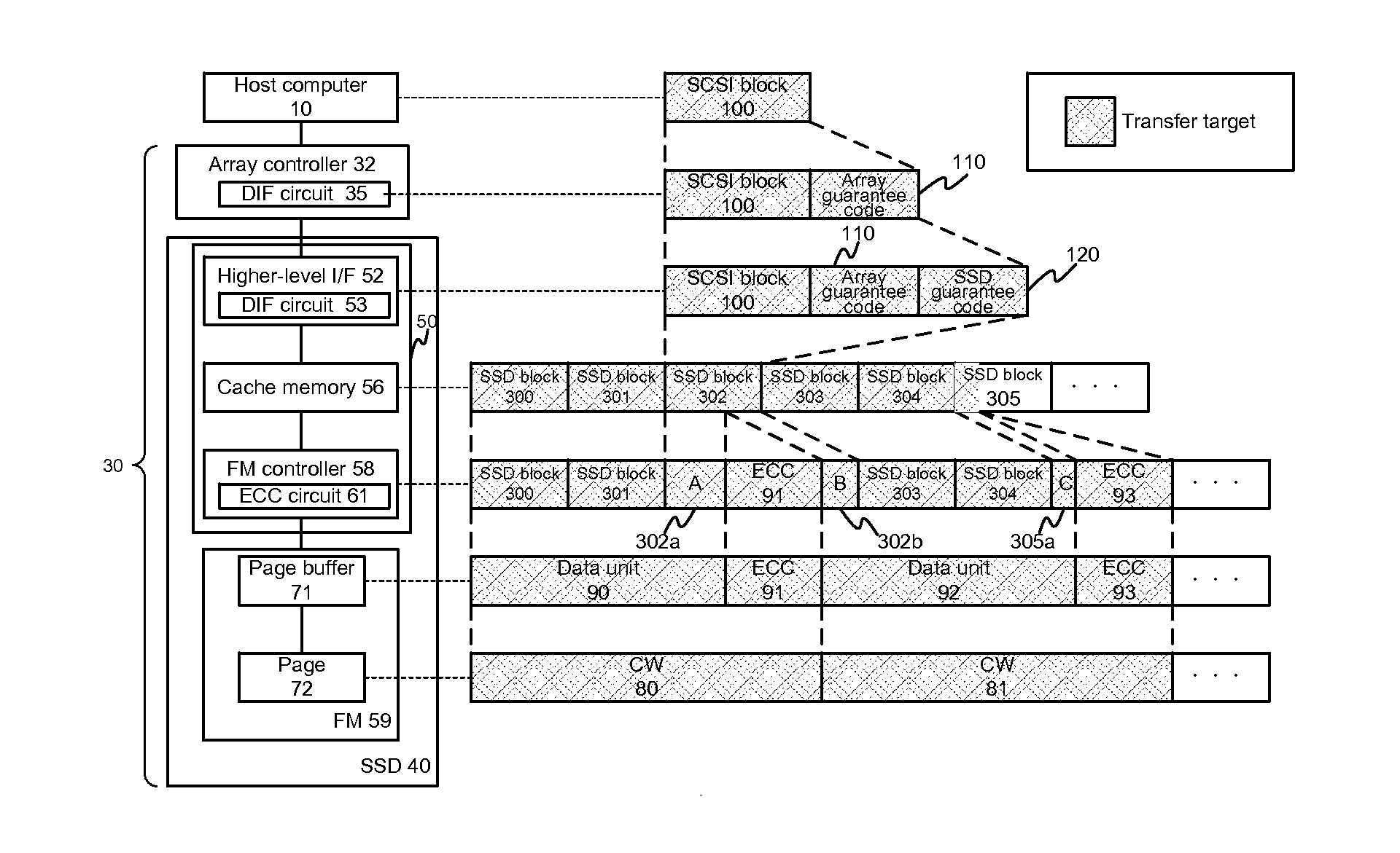
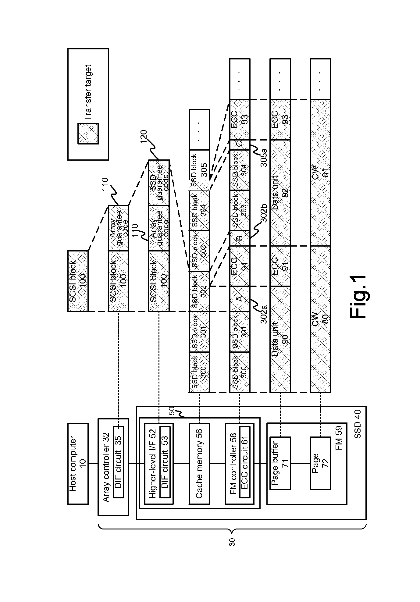
[0031]FIG. 1 shows an example of the correspondence relationship of the configuration of a storage system and the configuration of a data block in a comparative example.

[0032]In this example, the storage system includes a host computer 10 and a storage apparatus 30. The storage apparatus 30 includes an array controller 32 and an SSD 40. The host computer 10, the array controller 32, and the SSD 40 exchange data according to the SCSI protocol. In the SCSI protocol, data is transferred in units of predetermined data blocks (hereinafter referred to as “SCSI blocks”). The size of one SCSI block is 512 bytes, for example. Hereinafter, a case where the host computer 10 transmits, as data for writing, a SCSI block 100 to the array controller 32 will be described.

[0033]The array controller 32 includes a data integrity field (DIF) circuit 35, for example. The DIF circuit 35 generates an array controller guarantee code (hereinafter referred to as “array guarantee code”) 110 for guaranteeing c...

example 2

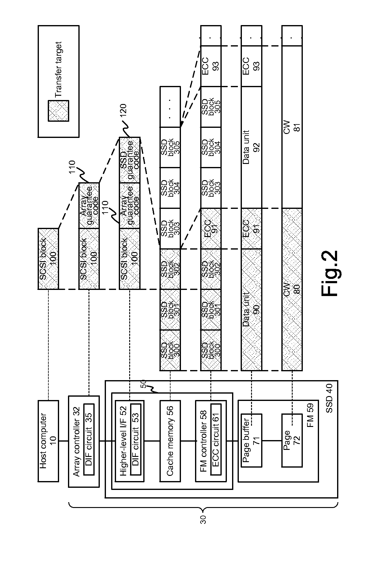
[0140]In a second example, a case where the SSD 40 performs compression of data inside will be described.

[0141]FIG. 16 shows an example of the correspondence relationship of the configuration of a storage system and the configuration of a data block according to the second example.

[0142]In comparison with the first example, the second example differs in that the SSD 40 includes the compression-decompression circuit 54 that performs compression and decompression of data. Thus, in comparison with the first example, the second example differs in sequence of transferring an SSD block between the cache memory 56 and the FM 59. Since data transfer between the host computer 10 and the array controller 32 is the same as in the first example, description is omitted herein.

[0143]Hereinafter, one example of a process in which the storage system according to the second example writes data will be described.

1) The SSD controller 50 adds the SSD guarantee code 120 to the array block 200 generated...


PUM


Abstract

In a storage apparatus including a storage medium including a plurality of pages as a unit of reading and writing data, a first data block including a data block received from a higher-level device is generated, a second data block of a predetermined size including one or more undivided first data blocks is generated, a third data block in which a correction code is added to the second data block is generated, the third data block is stored in a page buffer, and one or more of the third data blocks stored in the page buffer is written in a page, which is a write destination, out of the pages of the storage medium.

Description

TECHNICAL FIELD[0001]The present invention relates to a technique of reading and writing data in a storage apparatus.BACKGROUND ART[0002]A storage apparatus compatible with a small computer system interface (SCSI) exchanges data in units of data blocks of, for example, 512 bytes.[0003]In recent years, there are storage apparatuses such as a solid state drive (SSD) that use a flash memory as a recording medium. With a NAND flash memory, data is read / written in units called “pages” of, for example, 8 kilobytes.[0004]Data being held in a flash memory is by nature prone to error. Therefore an error correcting code (ECC) is added. A set of data stored in a flash memory and an ECC with respect to the data is referred to as code word (CW) (PTL 1 and PTL 2).CITATION LISTPatent Literature[PTL 1][0005]U.S. Pat. No. 8,103,936[PTL 2]US2011 / 0320915SUMMARY OF INVENTIONTechnical Problem[0006]In the case of reading data from a storage apparatus including a flash memory, it is necessary to execute a...

Claims


Application Information

Patent Timeline
Patent Type & Authority Applications(United States)
IPC IPC(8): G06F11/10G06F3/06G11C29/52
CPCG06F11/1068G06F3/0619G11C29/52G06F3/0679G06F3/064G06F11/1076G06F12/0246G06F12/04G06F12/16G06F2211/1014G06F2212/214G06F2212/403G06F2212/7202G06F2212/7208
Inventor KOSEKI, HIDEYUKITSUNEHIRO, TAKASHIOGAWA, JUNJIMIZUSHIMA, NAGAMASAKAWAMURA, ATSUSHI
Owner HITACHI LTD
Why Eureka
Try Eureka