Heat treatment apparatus and heat treatment method

a heat treatment apparatus and heat treatment technology, applied in the direction of electric heating, microwave heating, electric/magnetic/electromagnetic heating, etc., can solve the problems of difficult control of a given in-plane heat amount, difficult uniform heat treatment of silicon thin film, low mobility and a mutual conductance, etc., to achieve uniform heat treatment

Inactive Publication Date: 2016-01-14
TOKYO ELECTRON LTD
View PDF2 Cites 6 Cited by
  • Summary
  • Abstract
  • Description
  • Claims
  • Application Information

AI Technical Summary

Benefits of technology

[0022]In accordance with the present invention, when the processing chambers are seen so as to overlap with each other from the perpendicular direction to the lengthwise direction of the processing chambers, phases of standing waves generated in the processing chambers do not coincide with each other. Therefore, a sum of amplitudes in the phases of the standing waves corresponding to the each part of the target object almost keeps a balance, so that the heat amount given by the standing waves can be uniformalized in each part of the target object. As a result, a uniform heat treatment can be performed onto the target object by using a microwave.

Problems solved by technology

However, a silicon thin film in an amorphous state (hereinafter, referred to as “amorphous silicon thin film”) has a problem that a mobility and a mutual conductance are low.
However, since a laser light easily interferes and a spot diameter is small, a control of a given in-plane heat amount is difficult.
Further, in a large silicon thin film, a uniform heat treatment is difficult to be performed on the silicon thin film, and a uniform crystallization is also difficult.
As a result, there arises a problem such as a threshold voltage value becoming non-uniform in the TFTs.
However, the introduced microwave is reflected at an inner wall surface forming the processing space, which results in generation of a standing wave in the processing space.
Accordingly, a uniform heat treatment of the amorphous silicon thin film becomes difficult.

Method used


Image

  • Heat treatment apparatus and heat treatment method
  • Heat treatment apparatus and heat treatment method
  • Heat treatment apparatus and heat treatment method

Examples


Embodiment Construction

[0035]Hereinafter, embodiments of the present invention will be described with respect to the accompanying drawings.

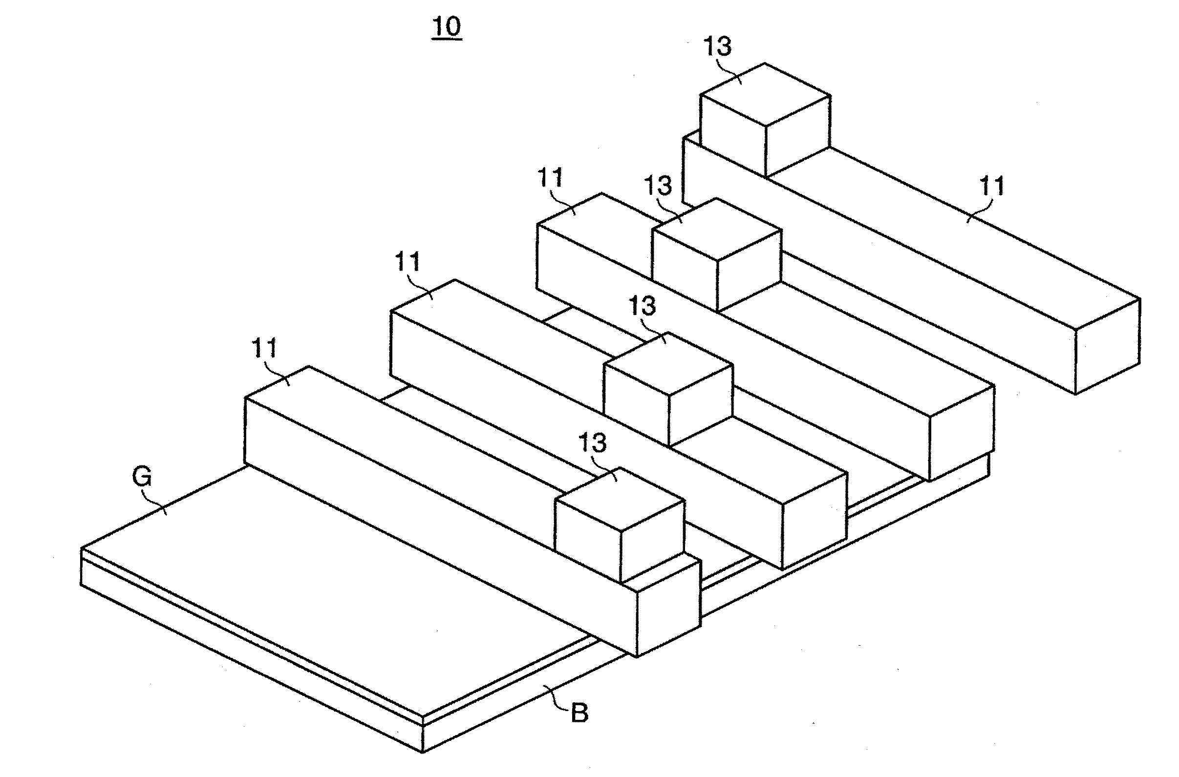
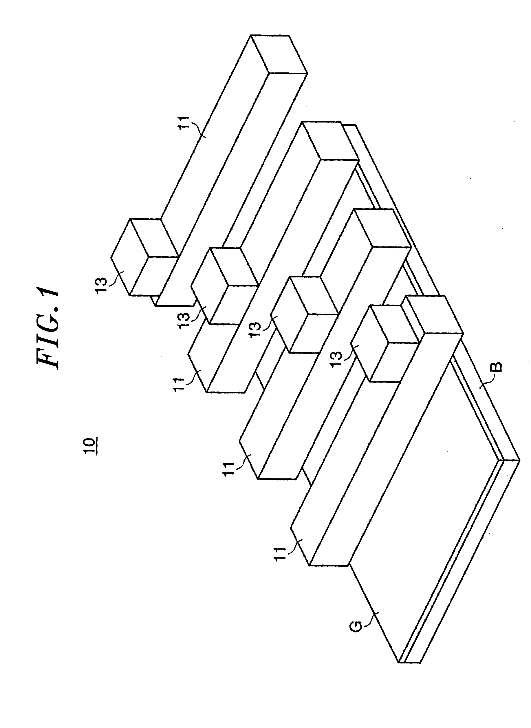
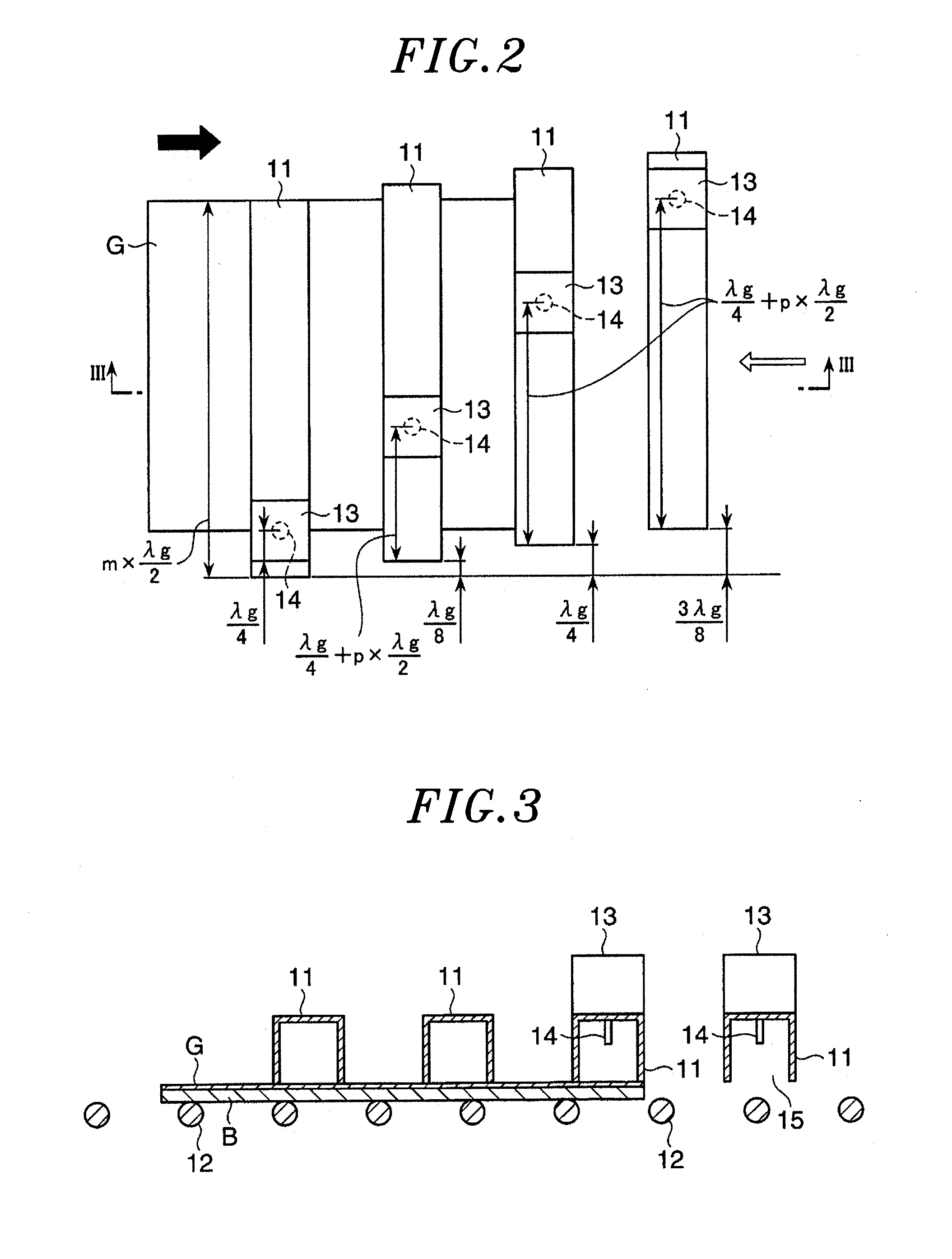
[0036]FIGS. 1 to 3 show a schematic configuration of a heat treatment apparatus in accordance with the present embodiment, wherein FIG. 1 is a perspective view, FIG. 2 is a plan view, and FIG. 3 is a cross-sectional view taken along with a line III-III of FIG. 2.

[0037]In FIGS. 1 to 3, a heat treatment apparatus 10 includes a plurality of tube-shaped processing chambers 11, and a plurality of rollers 12 arranged below the processing chambers 11 to be opposite to the processing chambers 11. The processing chambers 11 are disposed parallel to each other in a lengthwise direction of the processing chambers (hereinafter, simply referred to as “lengthwise direction”) and disposed at a substantially regular interval in a perpendicular direction to the lengthwise direction. The rollers 12 transfer a plate-shaped susceptor B made of a metal and a substrate G mounted on the susc...


PUM

PropertyMeasurementUnit
thicknessaaaaaaaaaa
frequencyaaaaaaaaaa
effective wavelengthaaaaaaaaaa

Abstract

A heat treatment apparatus includes processing chambers into which microwaves with an effective wavelength of λg are introduced. The processing chambers are arranged parallel to each other. The length from an inner wall surface of one end of each processing chamber in the lengthwise direction to an inner wall surface of the other end thereof is m×λg / 2 (m being a positive integer). An antenna sending microwave oscillation into the processing chambers is separated by λg / 4+p×λg / 2 (p being a positive integer including 0) from the inner wall surface of the end part in the lengthwise direction of each processing chamber. The processing chambers are disposed to be offset by λg / (2×n) (n being the number of the processing chambers) from each other in the lengthwise direction, when the processing chambers are seen to overlap with each other in a perpendicular direction to the lengthwise direction of each processing chamber.

Description

CROSSREFERENCE[0001]This application is a National Stage Application of, and claims priority to, PCT Application No. PCT / JP2013 / 085335, filed on Dec. 26, 2013, entitled “HEAT TREATMENT APPARATUS AND HEAT TREATMENT METHOD,” which claims priority to Japanese Patent Application No. 2013-037138, filed on Feb. 27, 2013. The foregoing patent applications are herein incorporated by reference by entirety for all purposes.FIELD OF THE INVENTION[0002]The present invention relates to a heat treatment apparatus and a heat treatment method that use a microwave.BACKGROUND OF THE INVENTION[0003]In a manufacturing process of a large panel such as a FPD (flat panel display) panel, PV (photovoltaics) panel or the like, a silicon thin film is formed in a large area on a surface of a large glass substrate by CVD (chemical vapor deposition). Then, a plurality of TFTs (thin-film transistors) or PIN diodes are formed by using the silicon thin film. Here, since the silicon thin film is formed on the glass ...

Claims


Application Information

Patent Timeline
Patent Type & Authority Applications(United States)
IPC IPC(8): H01L21/02H05B6/70H05B6/78H05B6/80
CPCH01L21/02667H05B6/70H01L21/02532H05B6/80H05B6/78H05B6/72H05B6/701H05B6/708H01L21/67115H01L21/6719H01L21/2686H01L21/02422H01L21/02631
Inventor KASAI, SHIGERUMIURA, HITOSHI
Owner TOKYO ELECTRON LTD
Why Eureka
Try Eureka