Transient Voltage Protection Circuits and Devices

a protection circuit and transient voltage technology, applied in the field of electronic circuits and devices, can solve the problems of limiting the area of integrated circuits (ics), limiting the size of esd protection circuits, and limiting the possibility of further reduction in the size of an i

Active Publication Date: 2016-01-14
INFINEON TECH AG
View PDF4 Cites 24 Cited by
  • Summary
  • Abstract
  • Description
  • Claims
  • Application Information

AI Technical Summary

Benefits of technology

[0007]According to an embodiment, a transient voltage protection circuit includes a first integrated circuit including an input node, an output node, a first transient voltage protection component coupled between the input node and a reference voltage node, and an impedance element coupled between the input node and the output node. The first transient voltage protection component has a first dynamic resistance and the output node is configured to be coupled to an electrostatic discharge (ESD) protection component having a second dynamic resistance that is greater than the first dynamic resistance.
[0008]In another embodiment, a method of protecting a circuit from a transient voltage includes providing a transient voltage protection circuit with an input node and an output node, receiving a transient peak current at the input node, conducting a major portion of the transient peak current to ground through a transient protection diode coupled to the input node, and conducting a minor portion of the transient peak current through a resistive element coupled between the input node and the output node. The output node is configured to be coupled to a device under protection (DUP) having a further transient voltage protection circuit. A dynamic resistance of the transient protection diode is less than a dynamic resistance of the further transient voltage protection circuit.
[0009]According to a further embodiment, a semiconductor device includes a substrate, a first electrostatic discharge (ESD) diode formed in the substrate, an insulating layer formed at a top surface of the substrate, a first contact layer formed at a top surface of the insulating layer, a first conductive layer formed in the insulating layer and coupling the first contact layer to the first ESD diode, a resistive layer formed in the insulating layer immediately adjacent to the first conductive layer, a second contact layer formed at the top surface of the insulating layer, a

Problems solved by technology

However, area on integrated circuits (ICs) is often limited.
Further, as some devices on ICs, such as logic circuitry, memory, and other circuitry are scaled to smaller geometries, the size of ESD protection circuits may not necessarily decrease in size.
ESD protect

Method used


Image

  • Transient Voltage Protection Circuits and Devices
  • Transient Voltage Protection Circuits and Devices
  • Transient Voltage Protection Circuits and Devices

Examples


Embodiment Construction

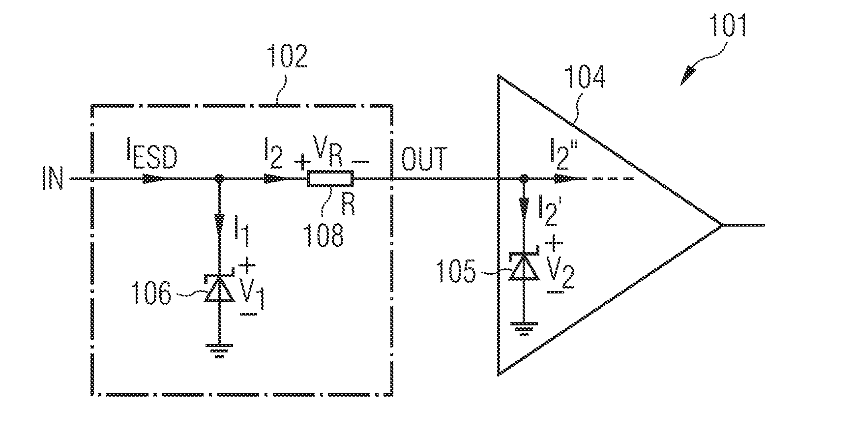
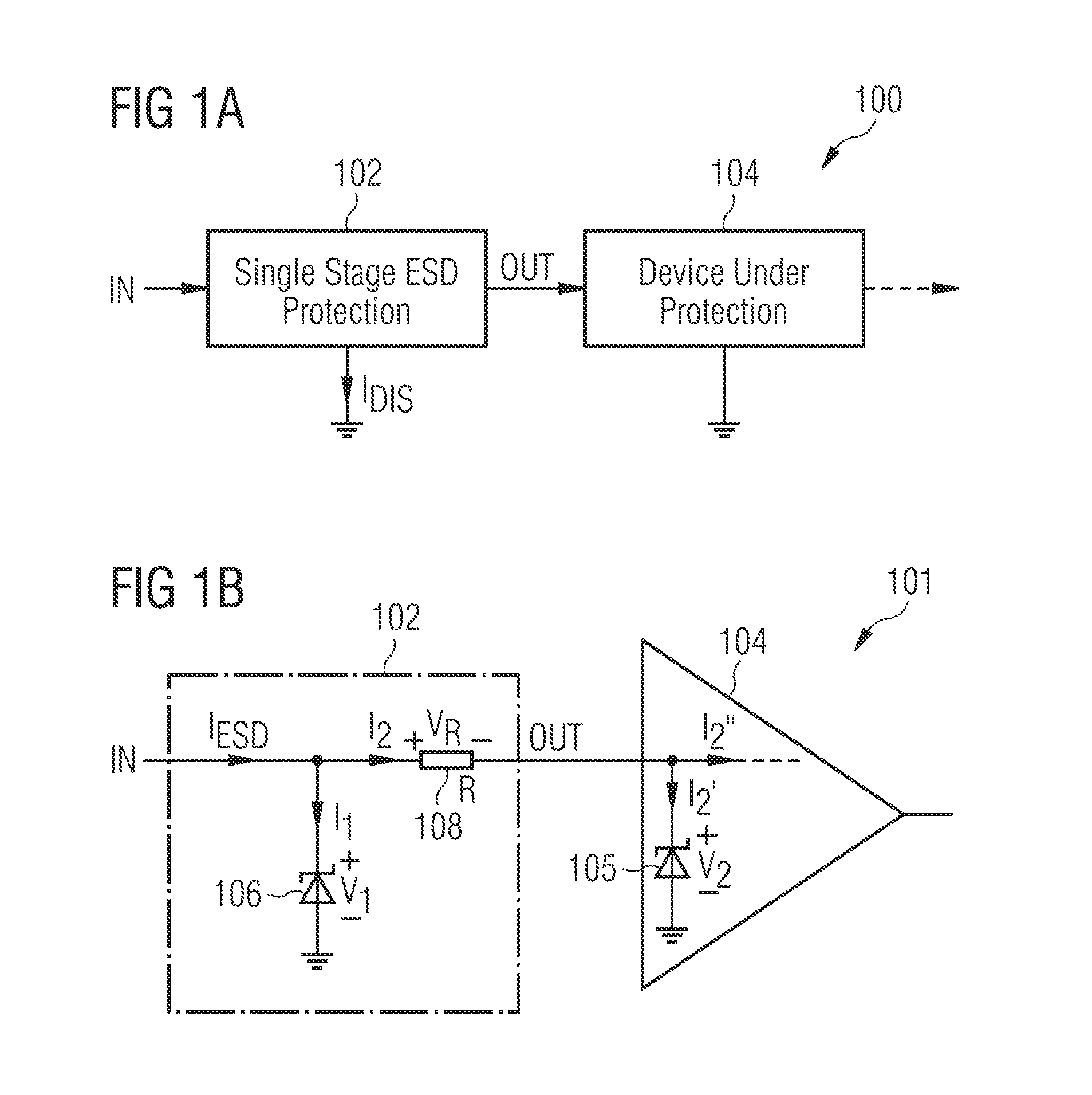
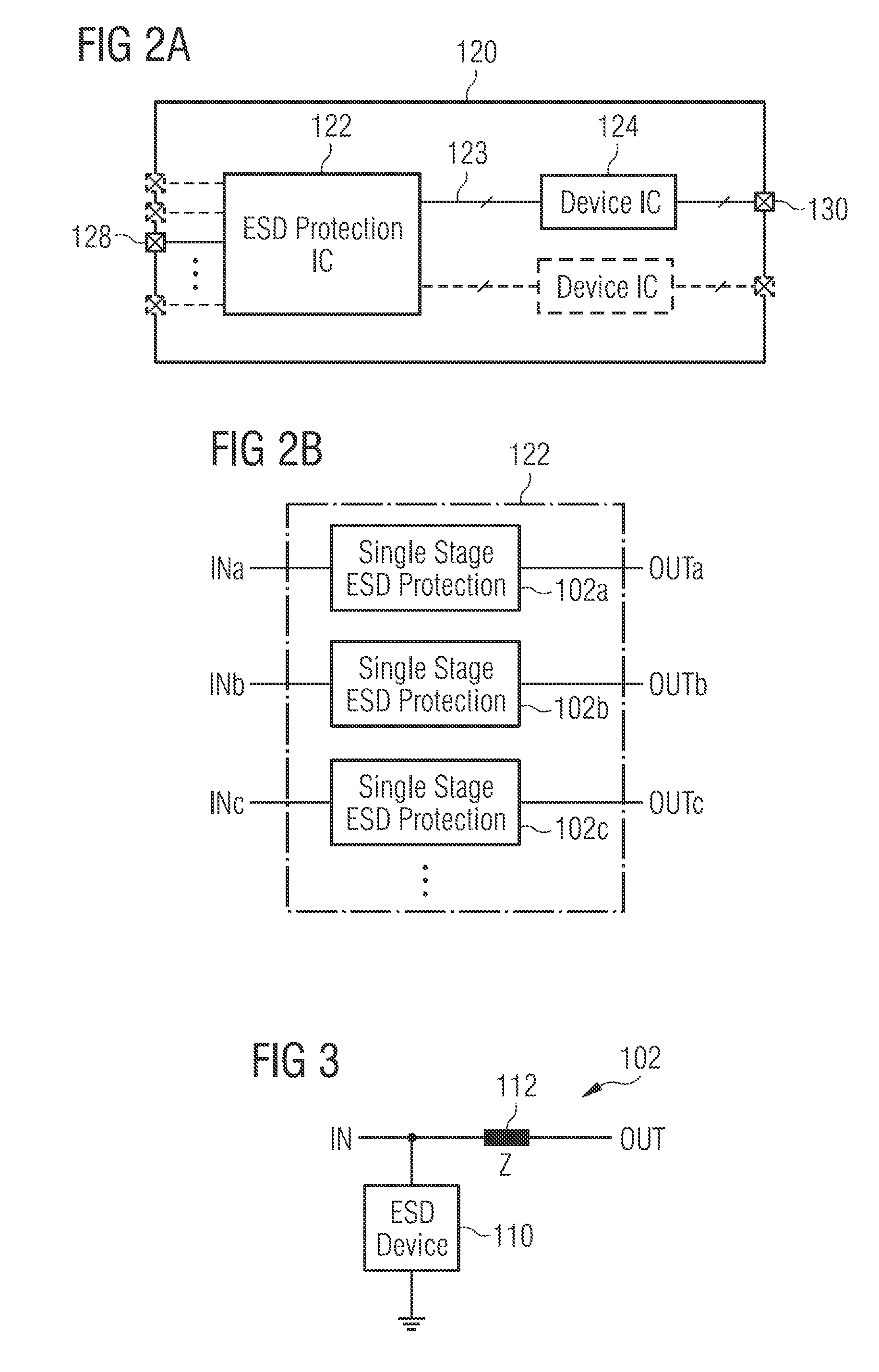
[0023]The making and using of various embodiments are discussed in detail below. It should be appreciated, however, that the various embodiments described herein are applicable in a wide variety of specific contexts. The specific embodiments discussed are merely illustrative of specific ways to make and use various embodiments, and should not be construed in a limited scope.

[0024]Description is made with respect to various embodiments in a specific context, namely integrated circuits (ICs), and more particularly, transient voltage, including electrostatic discharge (ESD) and surge event, protection devices and circuits. Some of the various embodiments described herein include ESD protection components, transient voltage suppression (TVS) diodes, and single stage ESD protection devices. In other embodiments, aspects may also be applied to other applications involving any type of ESD circuit according to any fashion as known in the art. Further, the terms transient voltage, ESD, and s...


PUM


Abstract

According to an embodiment, a transient voltage protection circuit includes a first integrated circuit including an input node, an output node, a first transient voltage protection component coupled between the input node and a reference voltage node, and an impedance element coupled between the input node and the output node. The first transient voltage protection component has a first dynamic resistance and the output node is configured to be coupled to an electrostatic discharge (ESD) protection component having a second dynamic resistance that is greater than the first dynamic resistance.

Description

TECHNICAL FIELD[0001]The present invention relates generally to electronic circuits and devices, and, in particular embodiments, to transient voltage protection circuits and devices.BACKGROUND[0002]Semiconductor devices are manufactured by depositing many different types of material layers over a semiconductor workpiece, wafer, or substrate, and patterning the various material layers using lithography. The material layers typically comprise thin films of conductive, semiconductive, and insulating materials that are patterned, etched, or altered to form integrated circuits (ICs). There may be a plurality of transistors, memory devices, switches, conductive lines, diodes, capacitors, logic circuits, and other electronic components formed on a single die or chip, for example.[0003]Many ICs include electrostatic discharge (ESD) protection circuits designed to protect the ICs against transient voltages such as ESD events and surges. An ESD protection circuit typically is designed to turn...

Claims


Application Information

Patent Timeline
IPC IPC(8): H02H9/04
CPCH02H9/04H02H9/046H01L27/0255H01L27/0248
Inventor GLAS, ALEXANDERSCHARNAGL, KLAUS
Owner INFINEON TECH AG
Why Eureka
Try Eureka