

Semiconductor component system with wireless interconnect and arrangements therefor
- Summary
- Abstract
- Description
- Claims
- Application Information
AI Technical Summary
Benefits of technology
Problems solved by technology
Method used
Image

Examples
Embodiment Construction
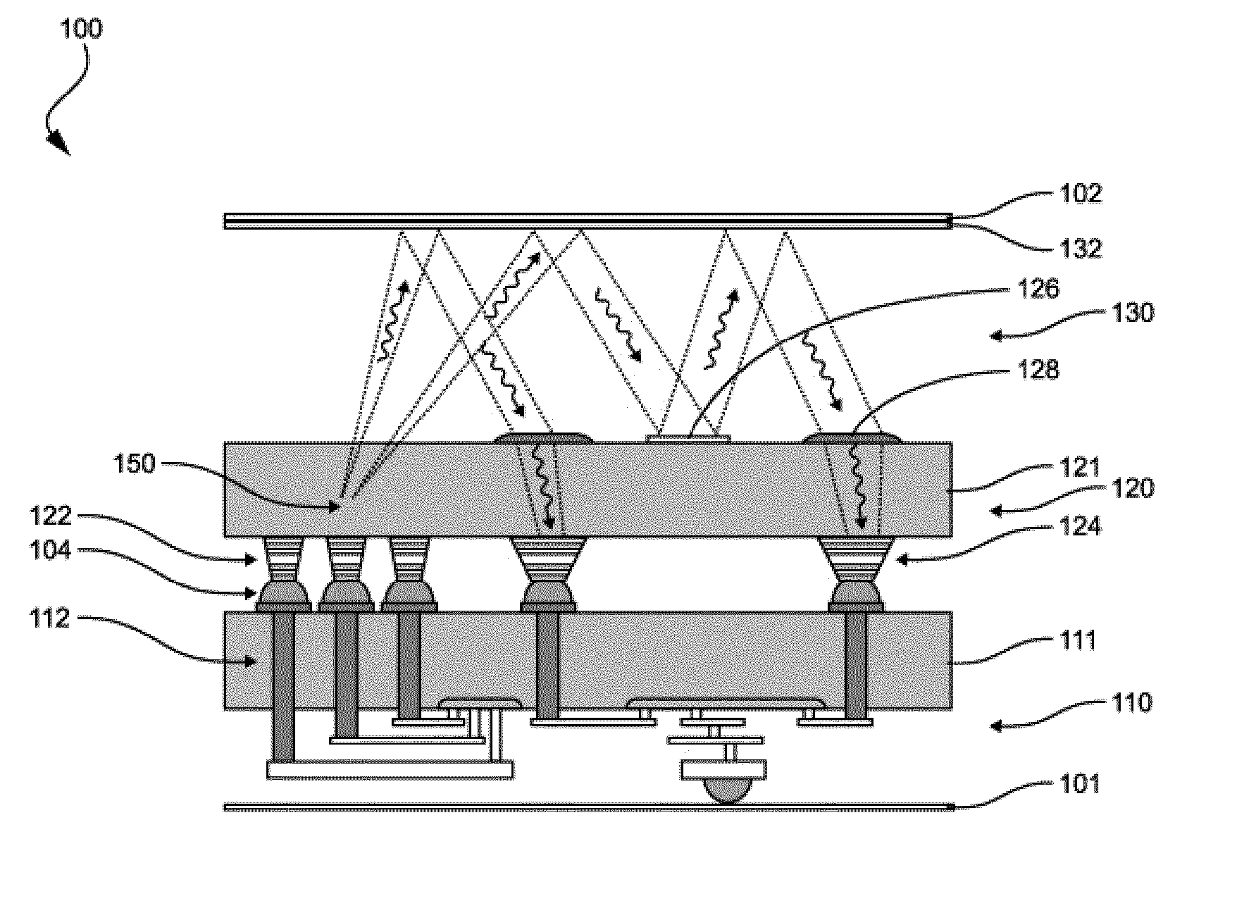
[0048]FIGS. 3A and 3B schematically illustrate a first preferred embodiment of an integrated semiconductor component system in a three-dimensional package 300. The integrated semiconductor component system 300 comprises a stack of processors 330 with single integrated semiconductor components on CMOS substrate layers 331 to 334, and a stack of random access memory devices 340 with single integrated semiconductor components on CMOS substrate layers 341 to 344.
[0049]By three-dimensional chip integration the single component layers 331 to 334 and 341 to 344 are horizontally connected with each other by the through-silicon via layers 302, 302, and 304, and superimposed on top of a package substrate by a flip-chip bonding layer 301 for example. The semiconductor component stacks 330, 340 are vertically connected with each other by the chip integration layer 305.
[0050]In this example, the stack of processors 330 also comprises transmitter modules 351 to 354 and receiver modules 361 to 364...
PUM
 Abstract
Description
Claims
Application Information