Light-emitting device, production method therefor, and device using light-emitting device

a technology of light-emitting devices and production methods, which is applied in the direction of semiconductor devices, electrical equipment, chemistry apparatus and processes, etc., can solve the problems that the conventional use of wirebonding methods is not desirable as a connection method, and achieve excellent flexural resistance or heat-cycle characteristics, prevent cracks or breakages, and improve adhesion

Active Publication Date: 2016-01-28
NICHIA CORP
View PDF17 Cites 28 Cited by
  • Summary
  • Abstract
  • Description
  • Claims
  • Application Information

AI Technical Summary

Benefits of technology

[0025]According to an embodiment of the present invention, there are provided: a light-emitting device that includes a light-transmissive electroconductive member comprising a light-transmissive electroconductive layer held on a light-transmissive insulator sheet, of which the light-transmissive electroconductive layer can hardly cause a crack or a fracture, that is excellent in flexural resistance or heat-cycle characteristic and that can hardly cause bubbles remaining therein, a process for production of the light-emitting device; and an apparatus including the luminescent device.
[0026]More specifically, the light-emitting device (or an apparatus including it) is characterized in that the sandwiching of a light-transmissive elastomer between an LED chip and a light-transmissive electroconductive layer, followed by hot pressing under vacuum, is effective for improving the adhesion between the light-transmissive elastomer and the transparent electroconductive member and preventing the occurrence of crack or breakage in the light-transmissive electroconductive layer, and also for partial intrusion of the elastomer between the electrode surface of the LED and the light-transmissive electroconductive layer to enhance the mechanical junction by the elastomer therebetween. As a result, even when the light-emitting device is subjected to severe bending or application of a heat cycle, the light-transmissive electroconductive layer does not readily cause a crack or a breakage, and a reliable electrical connection between the light-transmissive electro-conductive layer and the LED chip electrode is ensured, to allow a persistent lighting under such severe conditions.
[0027]Moreover, as the elastomer is processed under vacuum while preventing the melt-fusion of the elastomer causing a low-viscosity state, the remaining of air bubbles in the resultant light-emitting device is prevented. If the hot pressing is performed under an atmospheric pressure or a slight degree of reduced pressure, air bubbles remain especially in the circumference of the LED chip within the resultant light-emitting device and the air bubbles compressed during the hot pressing are liable to swell after the hot pressing, thus being further liable to cause a peeling between the LED chip electrode and the light-transmissive electroconductive layer. Furthermore, if the elastomer inserted between the LED tip and the light-transmissive electroconductive layer is melted or in a low-viscosity state at the time of the hot pressing, the LED chip is liable to be displaced or inclined to cause an electrical connection failure.

Problems solved by technology

As the connection method, the wirebonding method has been used conventionally but is not desirable as a connection method for use in a device requiring translucency, such as a touch panel or a light-emitting device.

Method used


Image

  • Light-emitting device, production method therefor, and device using light-emitting device
  • Light-emitting device, production method therefor, and device using light-emitting device
  • Light-emitting device, production method therefor, and device using light-emitting device

Examples


first embodiment

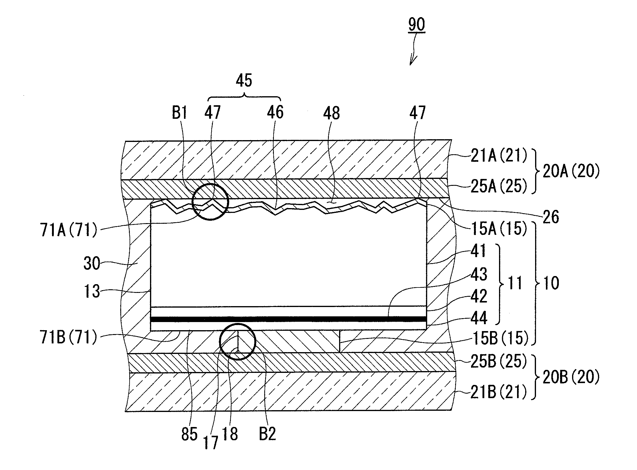
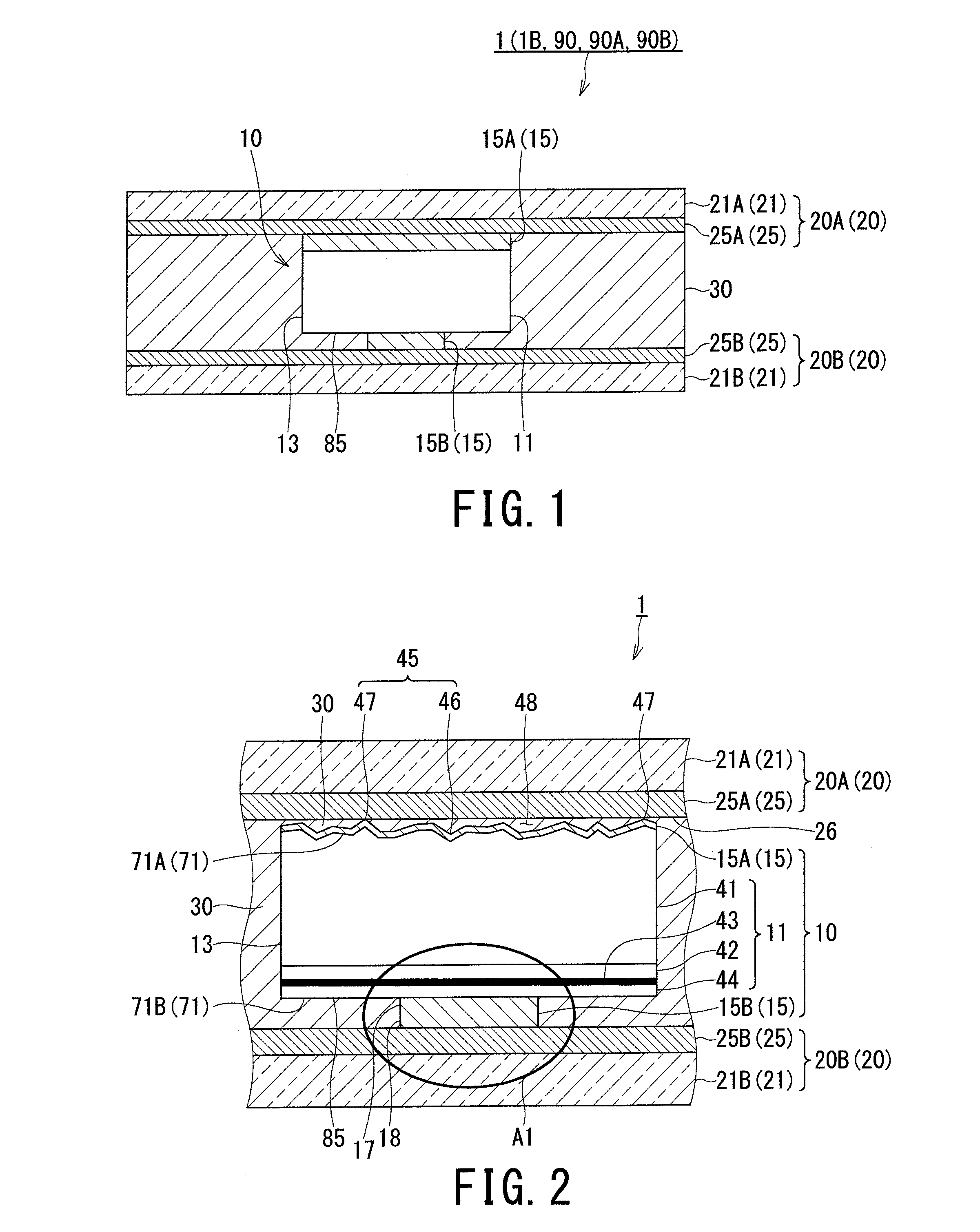
[0052]FIG. 1 is a sectional view of an essential part of a light-emitting device according to a first embodiment.

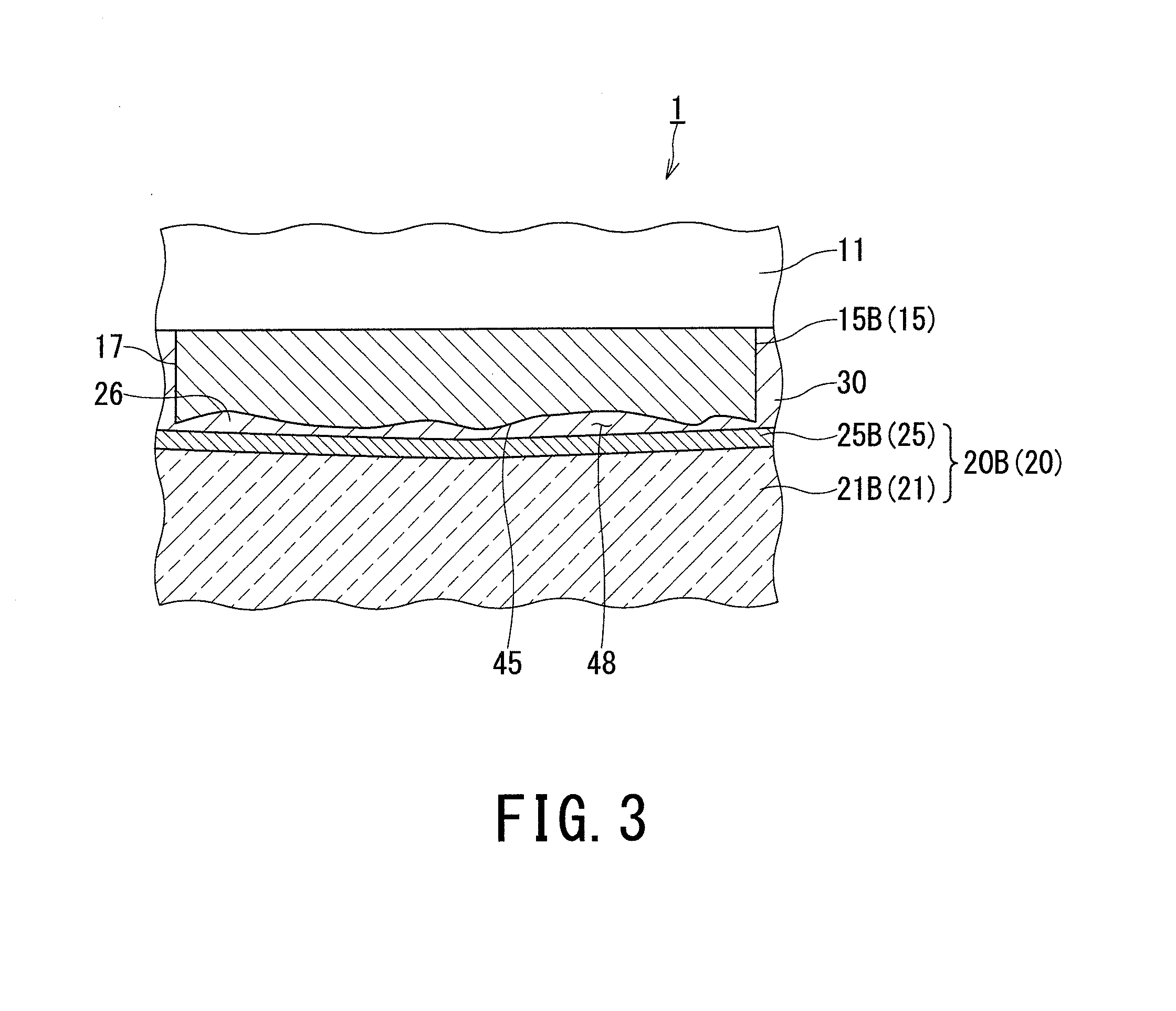
[0053]A light-emitting device 1, includes: an LED chip 10 including an LED body 11 and first and second electrode layers 15 (15A, 15B) formed on a front and a back face, respectively, of the LED body 11; first and second light-transmissive electroconductive members 20 (20A, 20B) respectively covering the LED chip 10 and including transparent substrates 21 (21A, 21B) and first and second light-transmissive electroconductive layers 25 (25A, 25B); and a light-transmissive elastomer layer 30 joined to a circumference 13 of the LED chip 10 and also to the light-transmissive electroconductive layer 25A of the light-transmissive electroconductive member 20A and the light-transmissive electroconductive layer 25B of the light-transmissive electroconductive member 20B.

[0054]In short, the light-emitting device 1 is formed by sandwiching the LED chip 10 with two sheets of the light-t...

second embodiment

[0147]FIG. 14 is a sectional view of a light-emitting device of a second embodiment. Compared with the light-emitting device 1 shown in FIG. 1 as a first embodiment, the light-emitting device 1A is different in that it includes an LED chip 10A having two types of electrodes 15A and 15B on one face thereof in place of the LED chip 10, a transparent substrate 21D having no light-transmissive electroconductive layer 25 in place of the first light-transmissive electroconductive member 20A, and a light-transmissive electroconductive member 20C having two types of light-transmissive electroconductive layers 25A and 25B in place of the second light-transmissive electroconductive member 20B, and the other structure is identical to the light-emitting device 1. Accordingly, with respect to the light-emitting device 1A shown in FIG. 14 as a second embodiment, the same components as those in the light-emitting device 1 shown in FIG. 1 as a first embodiment are denoted by identical symbols or nu...

example 1

Two-Face Electrode-Type LED Device

[0227]A strip-shaped LED device having a general structure including a length of about 90 mm and a width of about 50 mm was prepared by disposing six two-face electrode-type LED chips connected in series and arranged in a straight line with a spacing of about 5 mm from each other and disposing a pair of elastomer sheets respectively over the two faces of electrodes, followed by sandwiching with a pair of light-transmissive electroconductive member sheets and hot vacuum pressing. A partial laminate structure thereof was similar as shown in FIGS. 1 and 2. Details thereof are described below.

(LED Chip)

[0228]As LED chips, GaAlAs / GaAs-based red luminescence LED chips (planar size: about 300×300 μm, whole thickness (height): 175 μm) having electrodes on both front and back faces, were provided. The electrode layers on both faces of each LED chip included a substrate side electrode layer (15A) comprising a 3.5 μm-thick Au layer electrically connected to an...


PUM


Abstract

A light-emitting device, including: a pair of light-transmissive insulator sheets each provided with a light-transmissive electroconductive layer, or a pair of alight-transmissive insulator sheet equipped with light-transmissive electroconductive layers and alight-transmissive insulter sheet free from a light-transmissive electroconductive layer, disposed opposite to each other so as to form a region between the pair; at least one light-emitting semiconductor element each provided with a cathode and an anode which are individually and electrically connected to one of the light-transmissive electroconductive layers, and a light-transmissive elastomer, disposed between the pair of light-transmissive insulator sheets so as to fill the region in combination; wherein the light-transmissive elastomer is present at least locally between the cathode and anode, respectively, of the light-emitting semiconductor element and the light-transmissive electroconductive layers, and the light-transmissive elastomer is also present at concavities of the cathode and anode surfaces.

Description

CROSS-REFERENCE TO RELATED APPLICATIONS[0001]This application is based on and claims the priorities of preceding Japanese patent application No. 2013-069988 filed on Mar. 28, 2013 and Japanese patent application No. 2013-069989 filed on Mar. 28, 2013, of which the benefits are claimed herein and the entire disclosures are incorporated herein by reference.TECHNICAL FIELD[0002]The embodiments relate to a light-transmissive light-emitting device equipped with light-emitting elements, its production method, and an apparatus using the light-emitting device.BACKGROUND ART[0003]A light-transmissive light-emitting device is formed by electrically connecting electrodes disposed on light-emitting elements to light-transmissive electroconductive layers on a substrate. As the connection method, the wirebonding method has been used conventionally but is not desirable as a connection method for use in a device requiring translucency, such as a touch panel or a light-emitting device.[0004]On the o...

Claims


Application Information

Patent Timeline
Patent Type & Authority Applications(United States)
IPC IPC(8): H01L33/54H01L33/38H01L33/56H01L33/62
CPCH01L33/54H01L33/38H01L2933/005H01L33/62H01L33/387H01L33/56H01L25/0753H01L2224/16225H01L2924/07811B32B17/10036H01L2924/00H01L2924/00014H01L2924/12041
Inventor MAKI, KEIICHI
Owner NICHIA CORP
Why Eureka
Try Eureka