Memory control device and a delay controller
a memory control device and delay controller technology, applied in climate sustainability, digital storage, instruments, etc., can solve problems such as system performance decline, and achieve the effect of not reducing the performance of the system
- Summary
- Abstract
- Description
- Claims
- Application Information
AI Technical Summary
Benefits of technology
Problems solved by technology
Method used
Image


Examples
first embodiment
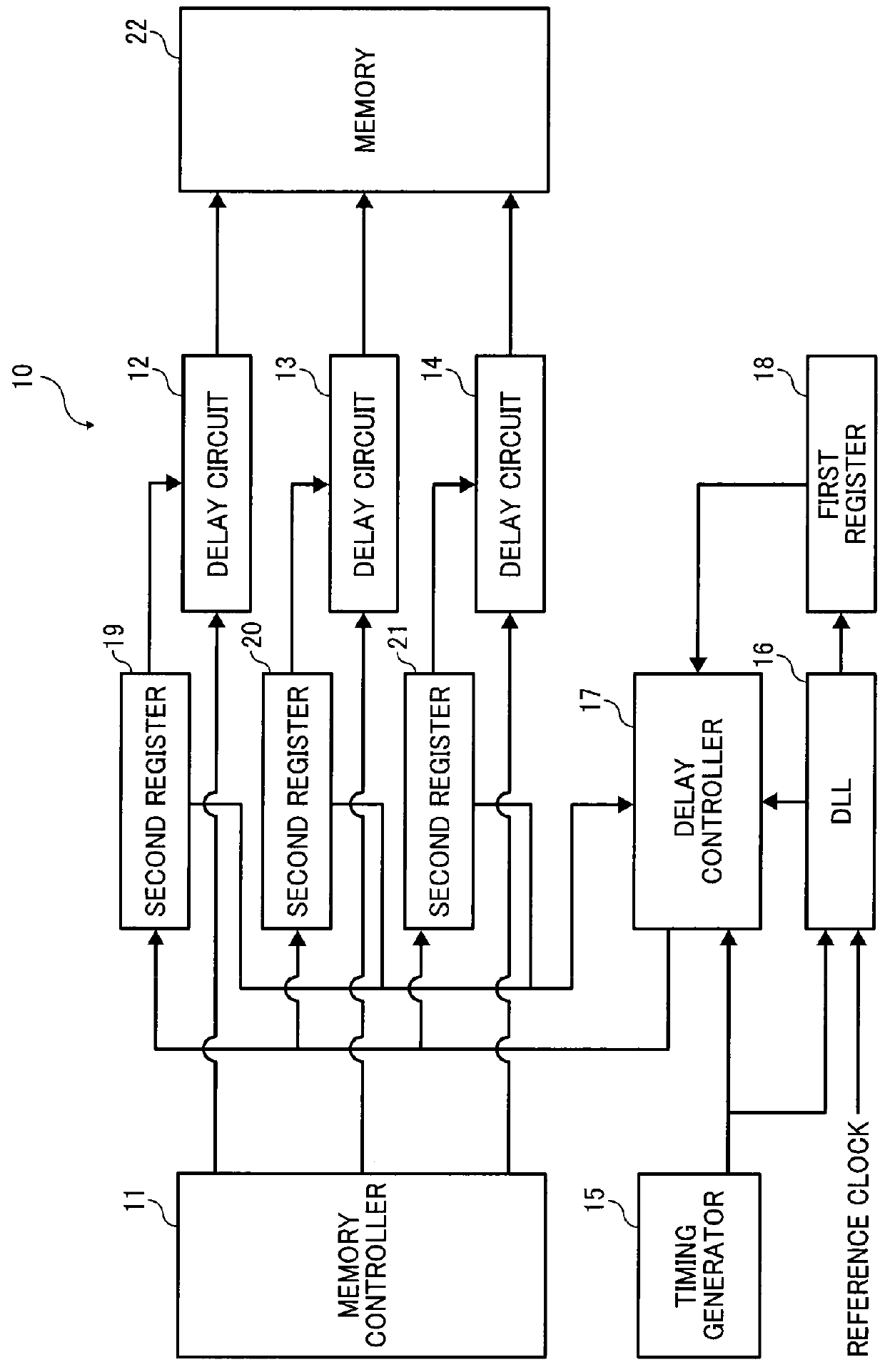
[0032]FIG. 1 is a block diagram showing the main configuration of the memory control device according to the The memory control device 10 includes a memory controller 11, delay circuits 12, 13, 14, a timing generator 15, a DLL circuit 16, a delay controller 17, a first register 18, second registers 19, 20, 21, and a memory 22.
[0033]The memory controller 11 is connected to each of the delay circuits 12, 13, 14. Further, the timing generator 15 is connecter to the delay controller 17 and the DLL circuit 16. The DLL circuit 16 is directly connected to the delay controller 17, and is indirectly connected to the delay controller 17 through the first register 18 by using another line.
[0034]The delay controller 17 is connected to each of the second registers 19, 20, 21. Moreover, the second registers 19, 20, 21 are respectively connected to the delay circuits 12, 13, and 14. In other words, the second register 19 is connected to the delay circuit 12, the second register 20 is connected to...
second embodiment
[0051]FIG. 2 is a block diagram showing the main configuration of the memory control device according to the
[0052]In the memory control device 30 of this embodiment, a timing generator 15 and the memory controller 11 are connected to each other, and a signal of a refresh flag is input to the timing generating circuit (generator) 15 from the memory controller 11.
[0053]Generally, since charges become zero and data disappears in the SDRAM by self-discharge, the SDRAM needs a refresh operation that electric charges are provided at regular intervals. The signal of the refresh flag is generated when a memory is refreshed. That is, this embodiment describes controlling the delay according to timing of refresh operation.
[0054]The timing generator 15 is configured to output a timing signal synchronized with the refresh cycle of the memory 22 based on the refresh flag (in other words, based on every refresh oparation) to the delay controller 17. Note that the other elements are the same as in...
third embodiment
[0062]FIG. 3 is a block diagram showing the main configuration of the memory control device according to the
[0063]In the present embodiment, a temperature sensor 35 is connected to the timing generator 15. An electrical signal (for example, a voltage or current) corresponding to the detected temperature at the temperature sensor 35 is input to the timing generating circuit (generator) 15. The other elements are the same as in the first embodiment.
[0064]In the present embodiment, the timing generator 15 controls the timing of the calibration execution of the DLL circuit 16 in response to the temperature value (the electrical signal) detected by the temperature sensor 35.
[0065]Since the amount of temperature change is proportional to the delay value, updating the delay value may not be needed if there is a small temperature change.
[0066]Thus, by using the temperature sensor 35, it is possible to reduce the number of executions of the DLL calibration and reduce power consumption. Note ...
PUM
 Abstract
Description
Claims
Application Information
 - R&D
- Intellectual Property
- Life Sciences
- Materials
- Tech Scout
- Unparalleled Data Quality
- Higher Quality Content
- 60% Fewer Hallucinations
Browse by: Latest US Patents, China's latest patents, Technical Efficacy Thesaurus, Application Domain, Technology Topic, Popular Technical Reports.
© 2025 PatSnap. All rights reserved.Legal|Privacy policy|Modern Slavery Act Transparency Statement|Sitemap|About US| Contact US: help@patsnap.com