Systems and methods for trimming control transistors for 3D NAND flash

Active Publication Date: 2016-02-04
MACRONIX INT CO LTD
View PDF0 Cites 7 Cited by
  • Summary
  • Abstract
  • Description
  • Claims
  • Application Information

AI Technical Summary

Benefits of technology

[0024]Described herein are methods for trimming control transistors for a memory array and systems for controlling the memory array using the trimmed control transistors. The memory array may have first and second strings of memory cells, and the control transistors may include first and second string select transistors,

Problems solved by technology

As discussed above, if the control transistors are not properly configured, a variety of problems can arise.
In general, an excessively low Vt can lead to slower programming speed, poor programming inhibition, and high leakage from unselected lines.
Conversely, an excessively high Vt can lead to read fails, as desired memory cells may not be fully selectable.
In some scenarios, uncontrolled threshold voltages may even lead to unintentional leakage between a common source line and a bit line, leading to degradation of the voltages on either or both lines.
As briefly mentioned above, various challenges affect the fabrication of 3D NAND Flash arrays.
If the memory cells utilize charge trapping technology such as silicon-oxi

Method used


Image

  • Systems and methods for trimming control transistors for 3D NAND flash
  • Systems and methods for trimming control transistors for 3D NAND flash
  • Systems and methods for trimming control transistors for 3D NAND flash

Examples


Embodiment Construction

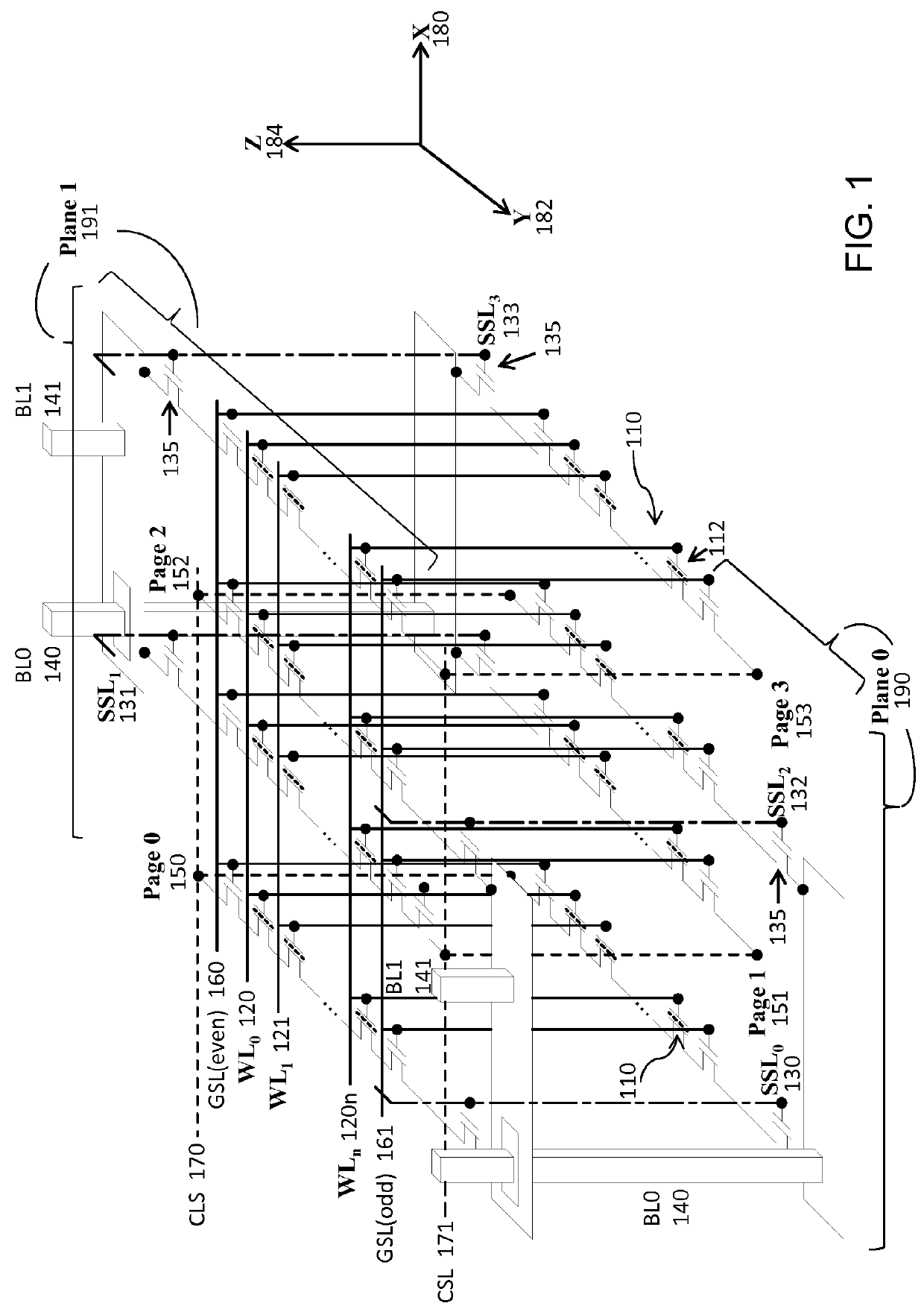
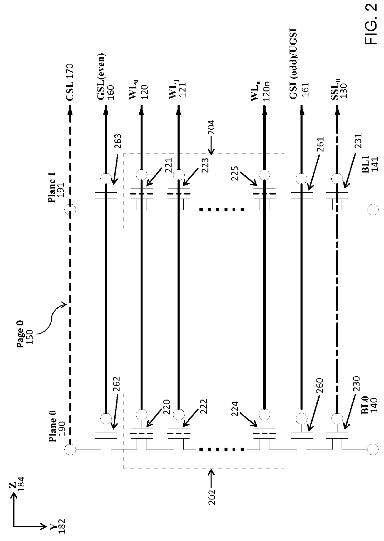
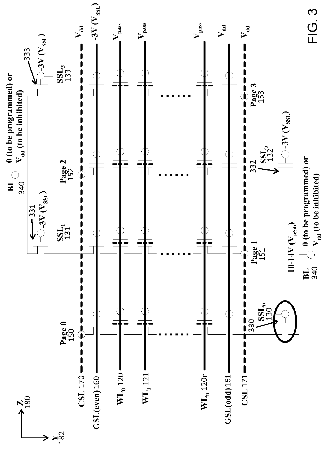
[0040]FIG. 3 shows a schematic view illustrating a string select transistor trimming action. The term “trimming” broadly refers to adjusting the Vt of one or more selected transistors. This trimming action is illustrated as being applied to a plane in the array structure shown in FIG. 1. Certain reference numerals are reused in FIGS. 3, 4, and 5 to represent structures similar to those previously presented and will not be described again.

[0041]During array operation, the string select transistors 330, 331, 332, 333 may each select a NAND string to be connected to a bit line 340. Generally, only one string is connected to the bit line 340 at a given time. It is therefore highly beneficial for the string select transistors 330, 331, 332, 333 to be predictably and reliably controllable. Accordingly, during the string select transistor trimming action, these transistors may each be trimmed individually. FIG. 3 specifically demonstrates the trimming of the string select transistor 330 in...


PUM


Abstract

Control transistors and memory cells within 3D NAND Flash memory arrays may both be created using the same technology, such as charge trapping structures, to simplify the fabrication process. However, the resulting control transistors may initially have higher variability in threshold voltages, when compared to traditional gate-oxide-based control transistors. Provided are exemplary techniques to trim control transistors to provide increased reliability and performance during array operation.

Description

RELATED APPLICATIONS[0001]The present application is related to U.S. patent application Ser. No. 13 / 078,311 entitled “Memory Architecture of 3D Array with Alternating Memory String Orientation and String Select Structures,” filed Apr. 1, 2011 and issued as U.S. Pat. No. 8,503,213 on Aug. 5, 2013, the contents of which are incorporated herein by reference.BACKGROUND[0002]1. Technical Field[0003]The present application generally relates to three-dimensional NAND Flash memory and, more specifically, to systems and methods of adjusting the threshold voltages of control transistors for better performance during operation of a memory array.[0004]2. Related Art[0005]NAND Flash memory is a nonvolatile memory that is used in a wide range of applications including mobile phones, digital cameras, and solid-state hard drives. The high storage density of NAND Flash memory, especially when compared to NOR Flash memory, has played a large role in its market penetration. This storage density is ach...

Claims


Application Information

Patent Timeline
IPC IPC(8): G11C16/10G11C16/04
CPCG11C16/10G11C16/0466G11C16/0483G11C16/08G11C29/028G11C29/024
Inventor CHANG, KUO PINCHANG, CHIH-SHENLUE, HANG-TING
Owner MACRONIX INT CO LTD
Why Eureka
Try Eureka