Memory circuit configuration schemes on multi-drop buses

a technology of memory circuit and configuration scheme, applied in memory adressing/allocation/relocation, digital storage, instruments, etc., to achieve the effect of improving efficiency and data throughput, preserving signal integrity, and reducing errors in writing data

Active Publication Date: 2016-02-11
QUALCOMM INC
View PDF6 Cites 9 Cited by
  • Summary
  • Abstract
  • Description
  • Claims
  • Application Information

AI Technical Summary

Benefits of technology

[0007]Aspects disclosed in the detailed description include memory circuit configuration schemes on multi-drop buses. In aspects disclosed herein, an on-die mapping logic is provided in a memory circuit. A memory controller communicates with the on-die mapping logic over a multi-drop bus. The on-die mapping logic is configured to receive a predetermined on-die termination (ODT) value from the memory controller. The predetermined ODT value will most often come in a multi-bit digital format from the memory controller, either as parallel bits or sequential bits. The predetermined ODT value is provided prior to reading from or writing to memory ranks of the memory circuit. In response to receiving the predetermined ODT value, the memory circuit sets on-die termination to the predetermined ODT value. The on-die mapping logic is further configured to instruct an on-die reference signal generator to generate a predetermined reference signal associated with the predetermined ODT value received from the memory controller. The predetermined reference signal provides an optimal reference voltage for implementing a desired equalization setting at the memory circuit. By dynamically adjusting the on-die termination and the predetermined reference signal, aspects of the present disclosure aid in preserving signal integrity. Such improved signal integrity reduces errors in writing data to the memory or in reading data from the memory circuit, thus leading to improved efficiency and data throughput on the multi-drop bus.

Problems solved by technology

While the latest versions of DDR SDRAM provide dynamic on-die termination, which allows the memory controller to reconfigure memory terminations independently depending on to which device the memory controller is currently writing, empirical evidence suggests that equalization methods suffer from the requirement for co-optimization for all potential connections, leading to a compromised solution, which is sub-optimal for any particular connection, albeit generally acceptable for all connections.

Method used


Image

  • Memory circuit configuration schemes on multi-drop buses
  • Memory circuit configuration schemes on multi-drop buses
  • Memory circuit configuration schemes on multi-drop buses

Examples


Embodiment Construction

[0020]With reference now to the drawing figures, several exemplary aspects of the present disclosure are described. The word “exemplary” is used herein to mean “serving as an example, instance, or illustration.” Any aspects described herein as “exemplary” is not necessarily to be construed as preferred or advantageous over other aspects.

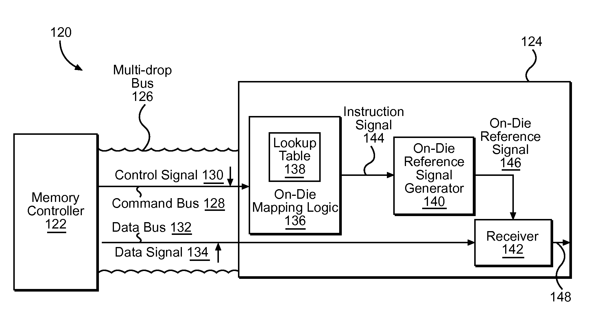
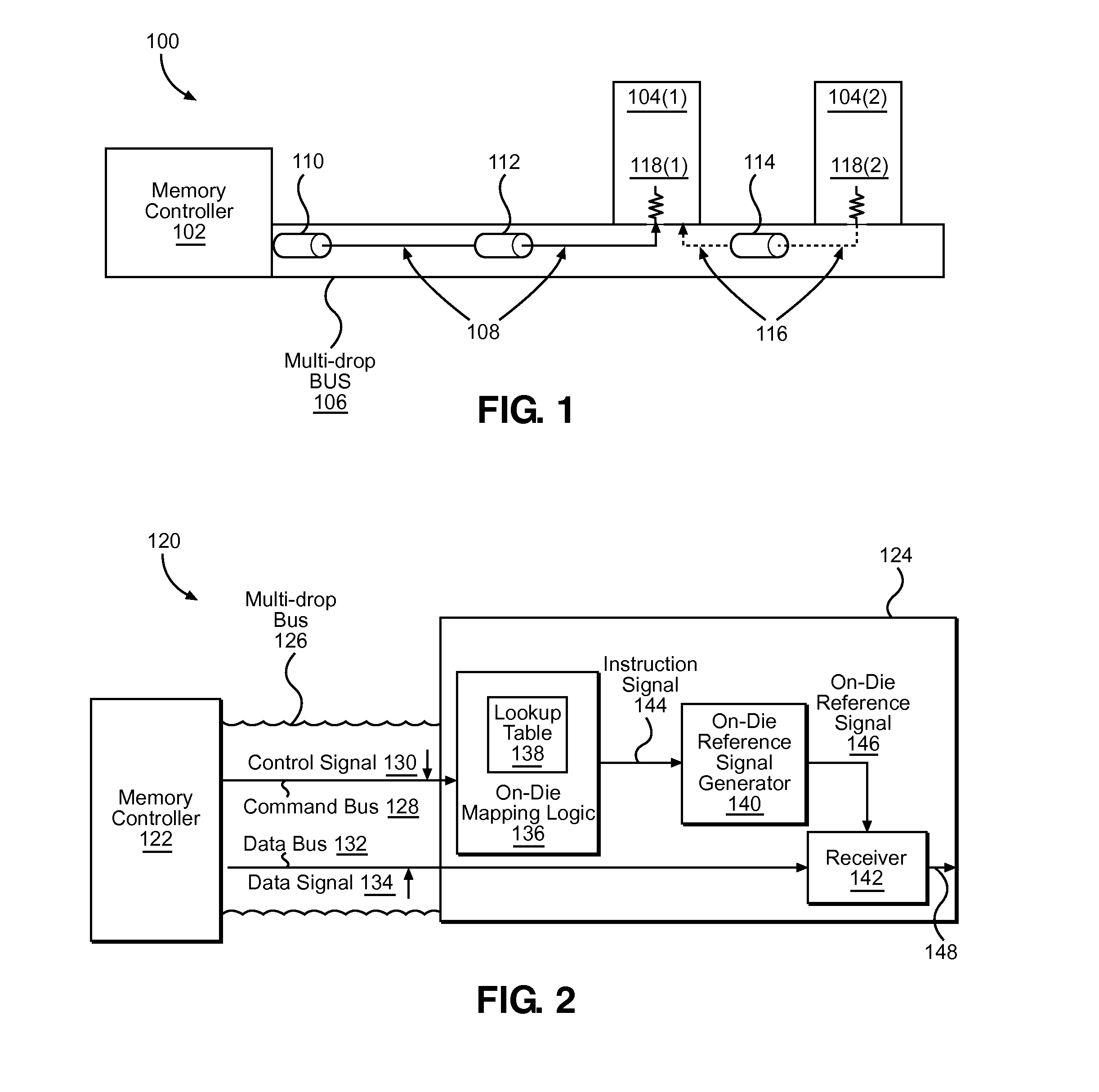
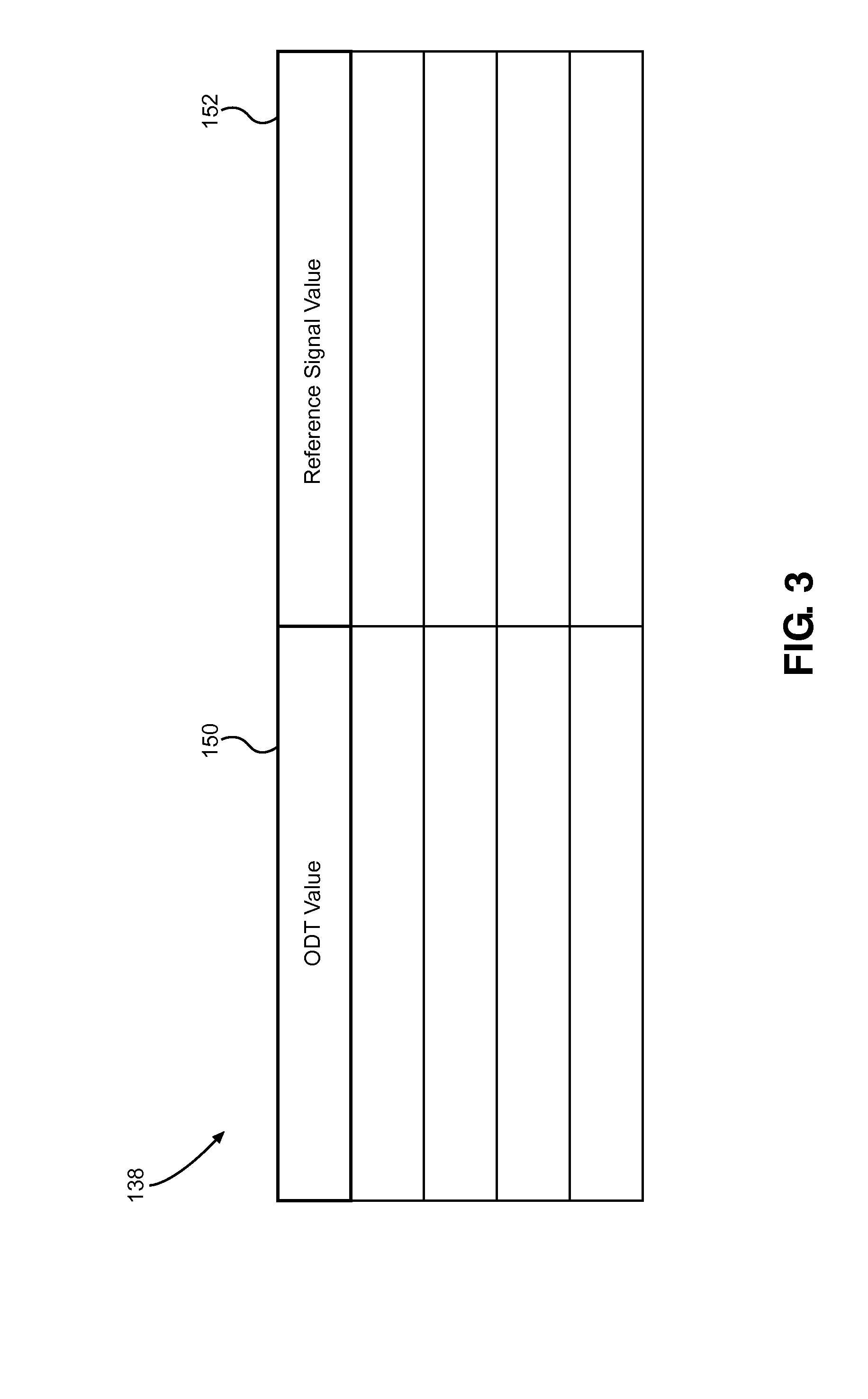
[0021]Aspects disclosed in the detailed description include memory circuit configuration schemes on multi-drop buses. In aspects disclosed herein, an on-die mapping logic is provided in a memory circuit. A memory controller communicates with the on-die mapping logic over a multi-drop bus. The on-die mapping logic is configured to receive a predetermined on-die termination (ODT) value from the memory controller. The predetermined ODT value will most often come in a multi-bit digital format from the memory controller, either as parallel bits or sequential bits. The predetermined ODT value is provided prior to reading from or writing to memory ranks of ...


PUM


Abstract

Memory circuit configuration schemes on multi-drop buses are disclosed. In aspects disclosed herein, an on-die mapping logic is provided in a memory circuit. A memory controller communicates with the on-die mapping logic over a multi-drop bus. The on-die mapping logic is configured to receive a predetermined on-die termination (ODT) value from the memory controller prior to being accessed. In response to receiving the predetermined ODT value, the memory circuit sets on-die termination to the predetermined ODT value and instructs an on-die reference signal generator to generate a predetermined reference signal associated with the predetermined ODT value. The predetermined reference signal provides an optimal reference voltage for implementing a desired equalization setting at the memory circuit, thus aiding in preserving signal integrity. Such improved signal integrity reduces errors in accessing the memory circuit, thus leading to improved efficiency and data throughput on the multi-drop bus.

Description

BACKGROUND[0001]I. Field of the Disclosure[0002]The technology of the disclosure relates generally to accessing circuits over a multi-drop bus.[0003]II. Background[0004]Modern electronic devices (e.g., computers, laptops, smartphones, etc.) all require a large amount of on-board memory for application processing and data storage needs. One type of on-board memory is known as a synchronous dynamic random access memory (SDRAM). Advancement of SDRAM technology has led to a class of high-density, high-throughput double data rate (DDR) SDRAM. The latest versions of DDR SDRAM include personal computer (PC) DDR-3, low-power (LP) DDR-3, PCDDR-4, and LPDDR-4. DDR SDRAM integrated circuits (ICs) are often packaged into an integrated memory module commonly referred to as a dual inline memory module (DIMM). Multiple DIMMs are usually needed to provide the large amount of on-board memory required by memory-consuming electronic devices.[0005]By design, a multi-drop memory bus is configured to pro...

Claims


Application Information

Patent Timeline
Patent Type & Authority Applications(United States)
IPC IPC(8): G06F13/42G06F12/10G06F13/16G11C7/10
CPCG06F13/4243G11C7/1072G06F2212/65G06F13/1694G06F12/1009G06F13/1689G11C7/1084G11C7/1093G11C7/22G11C11/4076G11C11/4093G11C29/025G11C29/028G11C2207/2254
Inventor HOLLIS, TIMOTHY, MOWRY
Owner QUALCOMM INC
Why Eureka
Try Eureka