Semiconductor device

a technology of semiconductors and circuits, applied in the direction of solid-state devices, basic electric elements, electric devices, etc., can solve the problems of increasing contact resistance or short-circuiting of wirings adjacent to contact parts, and achieve the effect of greater depth of focus

Active Publication Date: 2016-02-11
LONGITUDE LICENSING LTD
View PDF2 Cites 0 Cited by
  • Summary
  • Abstract
  • Description
  • Claims
  • Application Information

AI Technical Summary

Benefits of technology

[0018]With the present invention, a greater depth of focus can be achieved with a combination of NA exceeding 1 produced by liquid immersion and an illumination shape such as for example dipole and cross-pole, employing the peripheral part of a light source.

Problems solved by technology

However, with increasing progress in miniaturization of wiring patterns, if contact parts are merely arranged at intervals of alternate wirings, the contact part may sometimes deviate from the wiring pattern, resulting in the problems of increased contact resistance or short-circuiting of wirings adjacent to the contact part.

Method used


Image

  • Semiconductor device
  • Semiconductor device
  • Semiconductor device

Examples


embodiment 1

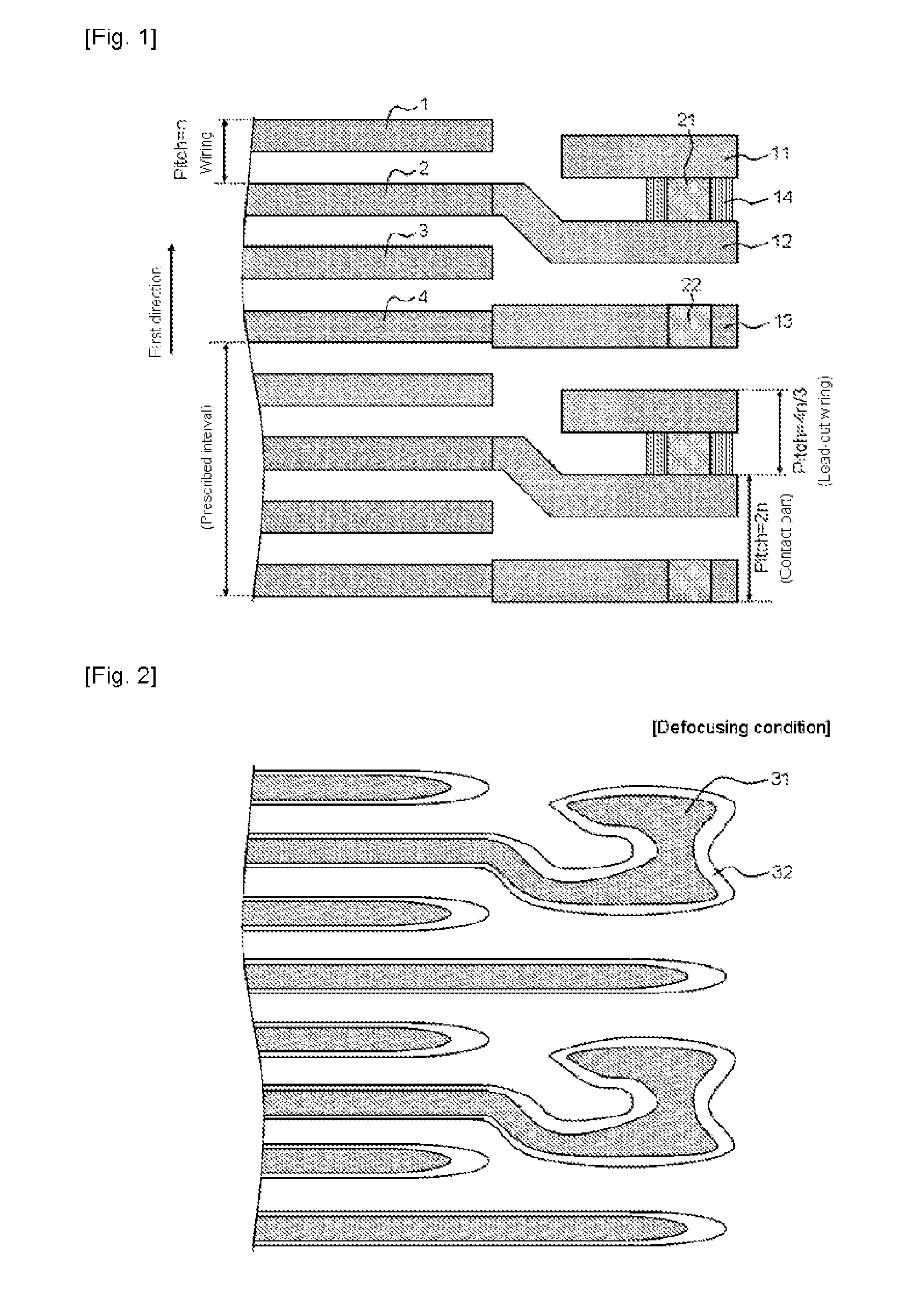
[0038]A semiconductor device according to Embodiment 1 of the present invention is described below with reference to the drawings. FIG. 1 is a plan view showing diagrammatically the layout pattern of the wiring of a semiconductor device according to Embodiment 1 of the present invention. FIG. 2 is a plan view showing diagrammatically a resolution pattern when the layout pattern of the wiring of a semiconductor device according to Embodiment 1 of the present invention is resolved under defocusing conditions.

[0039]Referring to FIG. 1, in this semiconductor device, in a wiring layer of multi-layer wiring structure, in which wirings and insulating layers are laminated, four wirings 1 to 4 are arranged in order from the top of FIG. 1 within a prescribed interval (4n times pitch) in a first direction, and the arrangement of wirings 1 to 4 is repeated. Wirings 1 to 4 extend in a direction at right angles to the first direction and have respectively the same wiring width; adjacent wirings 1...

embodiment 2

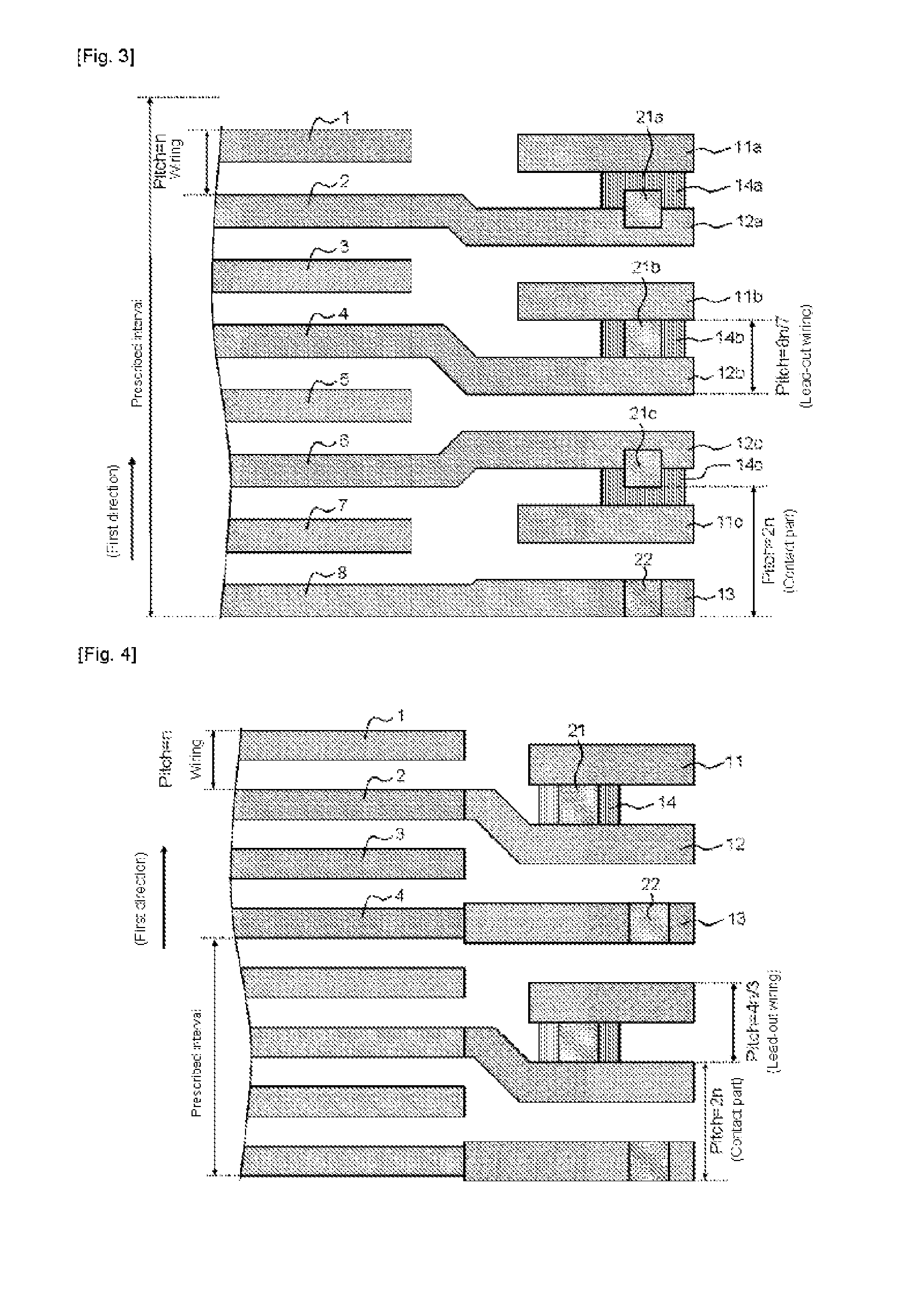
[0044]A semiconductor device according to Embodiment 2 of the present invention is described below with reference to the drawings. FIG. 3 is a plan view showing diagrammatically the layout pattern of the wiring of a semiconductor device according to Embodiment 2 of the present invention.

[0045]Embodiment 2 is a modification of Embodiment 1, in which lead-out wiring parts 11a, 12a, 11b, 12b, 12c, 11c, and 13 are arranged with 8 / 7 times pitch.

[0046]Referring to FIG. 3, in a semiconductor device, in a wiring layer of multi-layer wiring structure in which wirings and insulating layers are laminated, within a prescribed interval (8n times pitch) in a first direction, eight wirings 1 to 8 are disposed in order from the top of FIG. 3; the arrangement of the wirings 1 to 8 is repeated. The wirings 1 to 8 extend in a direction at right angles to the first direction and are respectively of the same wiring width, adjacent wirings 1 to 8 being mutually separated with an interval that is the same...

embodiment 3

[0051]A semiconductor device according to Embodiment 3 of the present invention is described below with reference to the drawings. FIG. 4 is a plan view showing diagrammatically the layout pattern of the wiring of the semiconductor device according to Embodiment 3 of the present invention.

[0052]Embodiment 3 is a modification of Embodiment 1, in which the bridge parts 14 between the lead-out wiring parts 11, 12 are arranged closer to the wirings 1 to 4 than the contact parts 22. Other aspects of the construction are the same as in the case of Embodiment 1.

[0053]The same beneficial effects as in the case of Embodiment 1 are presented by Embodiment 3.

[0054]It should be noted that, in the present application, where reference numerals are provided in the drawings, these serve merely for assisting comprehension and are not intended to be restricted to the illustrated embodiments.

[0055]Also, within the compass of the entire disclosure (including the claims and drawings) of the present inve...


PUM


Abstract

One semiconductor device includes first to fourth wirings disposed within a prescribed interval in a first direction, extending in a second direction, and arranged at a first pitch in the first direction, first to third lead-out wirings disposed within the prescribed interval in the first direction, extending in the second direction, and arranged at a second pitch in the first direction, a bridge part disposed between the first lead-out wiring, and the second lead-out wiring, and connected to the first lead-out wiring, and the second lead-out wiring, a first contact part in contact with at least one part of the bridge part, and a second contact part in contact with the third lead-out wiring. One of either the first lead-out wiring, or the second lead-out wiring is connected to the second wiring, and the third lead-out wiring is connected to the fourth wiring.

Description

TECHNICAL FIELDDetails of Related Applications[0001]The present invention claims priority from: Japanese Patent Application Number 2013-081409 (filed on Apr. 9, 2013), the entire disclosure of which application is incorporated in the present specification by way of reference.[0002]The present invention relates to a semiconductor device and in particular relates to a semiconductor device having a layout pattern of wiring that is electrically connected with a contact part.TECHNICAL BACKGROUND[0003]In the lithographic technique of manufacturing semiconductor devices, reduction of the optical pitch of the contact hole pattern tends to be more difficult to achieve than in the case of the wiring pattern: typically when providing a contact part 121 on a periodic pattern such as that of wirings 101, 102 of FIG. 5, the contact part connected therewith is constituted with a pitch of twice that of the wirings 101, 102 in question. However, with increasing progress in miniaturization of wiring ...

Claims


Application Information

Patent Timeline
Patent Type & Authority Applications(United States)
IPC IPC(8): H01L23/528
CPCH01L23/528H01L23/522H01L2924/0002H01L21/0274H01L2924/00H01L21/0337
Inventor ASANAO, SHUNSUKE
Owner LONGITUDE LICENSING LTD
Why Eureka
Try Eureka