
Positive resist composition and patterning process
a composition and resist technology, applied in the field of positive resist composition and patterning process, can solve the problems of difficult to satisfy both resolution and circularity in the formation of contact hole patterns, the control of dissolution is a problem, and the difficulty in satisfying both resolution and circularity, etc., to achieve excellent pattern profile, excellent depth of focus characteristics, and excellent resolution
- Summary
- Abstract
- Description
- Claims
- Application Information
AI Technical Summary
Benefits of technology
Problems solved by technology
Method used
Image

Examples
examples
[0067]Hereinafter the present invention will be explained specifically by showing Examples and Comparative Examples. However the present invention is not restricted by these descriptions.
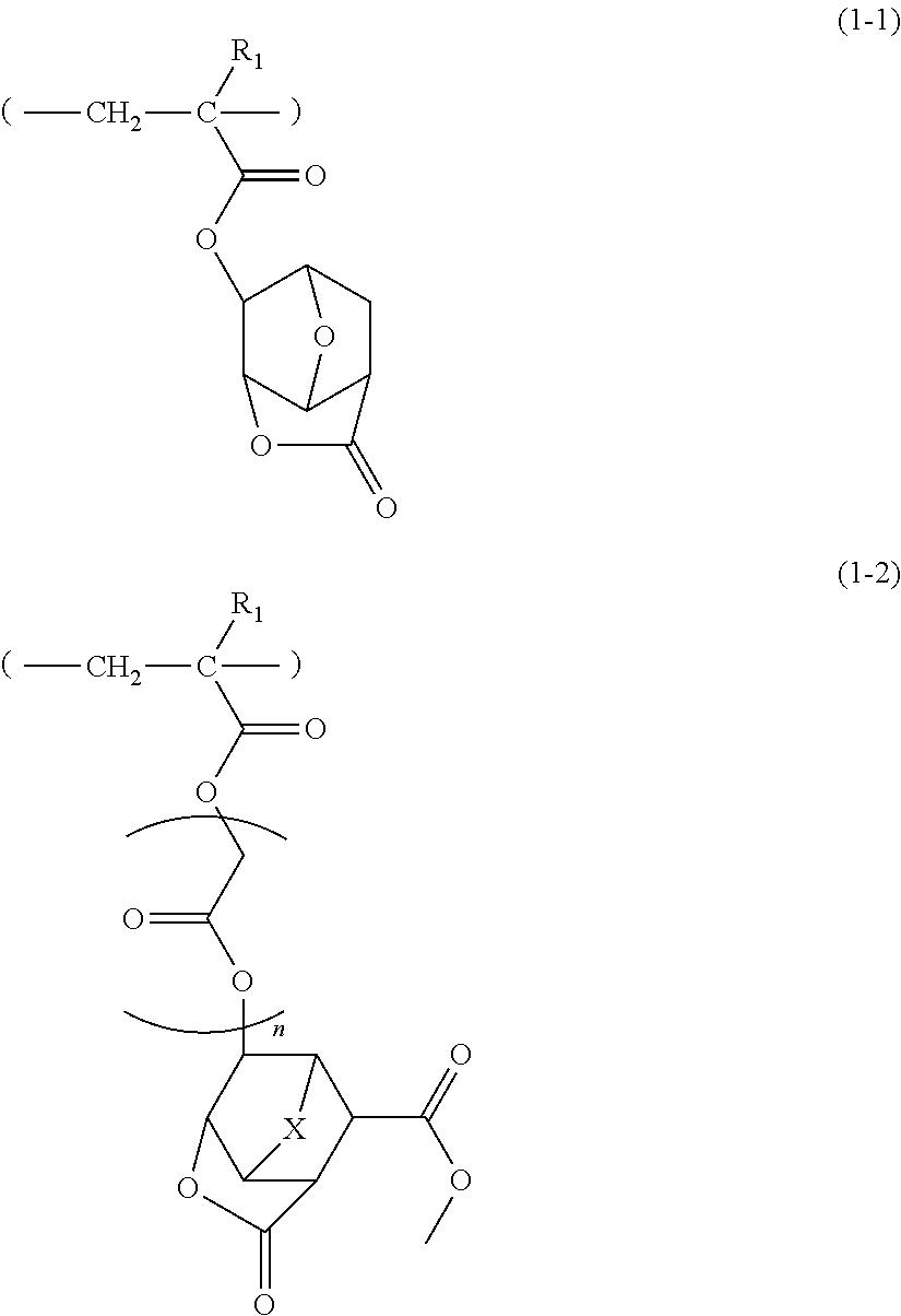
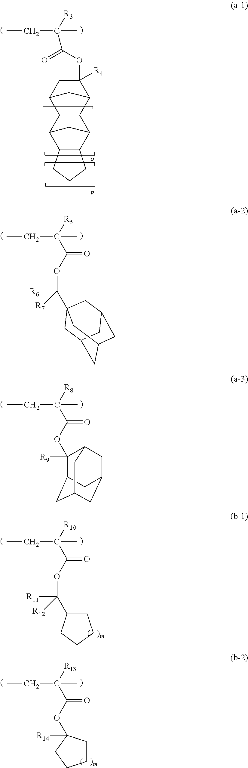
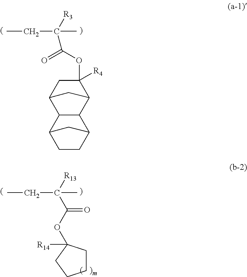
[0068]Composition ratios (% by mole) of repeating units to constitute the resin and molecular weight (Mw) thereof are shown in Table 1. Meanwhile, molecular weight (Mw) is the weight-average molecular weight in terms of polystyrene equivalent measured with GPC. In addition, structures of respective repeating units are shown in Table 2 and Table 3.
[0069]Meanwhile, Polymer-17 and Polymer-18 are the resins not containing the repeating units shown by the general formulae (a-1) to (a-3); Polymer-26 and Polymer-30 are the resins containing neither the repeating units shown by the general formulae (b-1) and (b-2) nor the repeating unit shown by the general formula (1-2); Polymer-27 is the resin containing neither the repeating units shown by the general formulae (a-1) to (a-3) nor the repeating unit shown ...
PUM
| Property | Measurement | Unit |
|---|---|---|
| wavelength | aaaaa | aaaaa |
| solubility | aaaaa | aaaaa |
| alkaline-solubility | aaaaa | aaaaa |
Abstract
Description
Claims
Application Information