Electron beam writing apparatus and electron beam writing method

a writing apparatus and electron beam technology, applied in the direction of photomechanical apparatus, beam deviation/focusing by electric/magnetic means, instruments, etc., can solve the problem of irradiation to a position deviating from a target position, and achieve the effect of reducing the width of the circuit line, reducing the number of circuit lines, and increasing the capacity of large-scale integrated

Active Publication Date: 2013-08-22
NUFLARE TECH INC
View PDF11 Cites 6 Cited by
  • Summary
  • Abstract
  • Description
  • Claims
  • Application Information

AI Technical Summary

Benefits of technology

[0003]The tendency in recent years towards higher mounting densities and larger capacities of large-scale integrated (LSI: Large Scale Integration) circuits are further reducing the circuit line widths needed for semiconductor devices.
[0004]Fabrication of semiconductor devices involves the use of photomasks or reticles (hereinafter, referred to collectively as masks) each having circuit patterns formed thereon. The circuit patterns on a mask are photolithographically transferred on to a wafer using a reduction projection exposure apparatus, often called a stepper, whereby the circuit patterns are formed on the wafer. An electron beam writing apparatus capable of writing fine patterns is used to manufacture the masks used to transfer the fine circuit patterns onto the wafer. This electron beam writing apparatus has inherently superior resolution, and can ensure greater depth of focus, thus allowing control over size fluctuations even with a difference in level.

Problems solved by technology

Accordingly, the electron beam drifts under the influence of the reflected electrons or the secondary electrons, which results in irradiation to a position deviated from a target position.

Method used


Image

  • Electron beam writing apparatus and electron beam writing method
  • Electron beam writing apparatus and electron beam writing method
  • Electron beam writing apparatus and electron beam writing method

Examples


Embodiment Construction

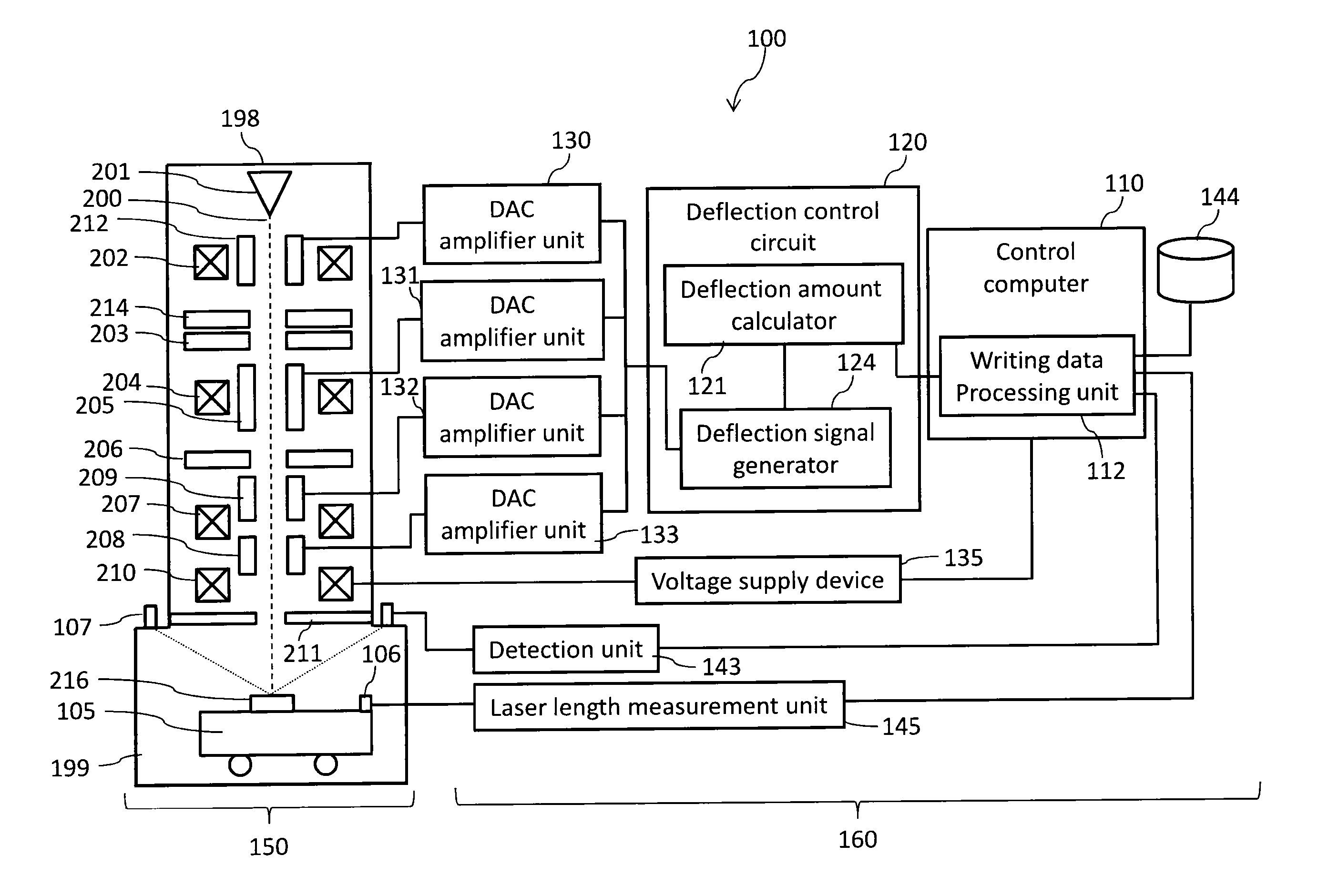
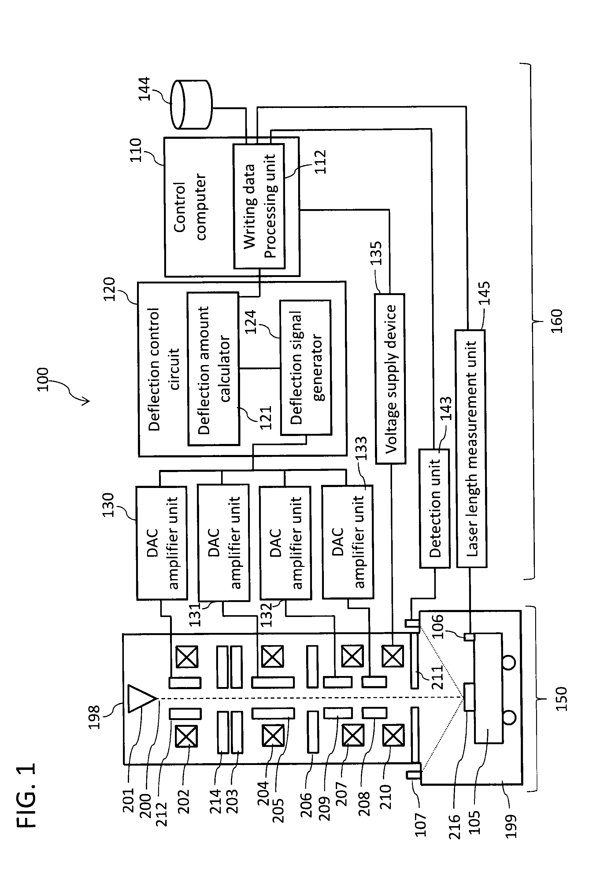
[0032]FIG. 1 is a schematic diagram of an electron beam writing apparatus according to an embodiment of the present invention.

[0033]The electron beam writing apparatus 100 consisting of a writing unit 150 and a control unit 160, is one example of a variable shape electron beam writing apparatus.

[0034]The writing unit 150 includes an electron optical column 198 and a writing chamber 199.

[0035]The electron optical column 198 includes an electron gun 201, an illumination lens 202, a blanking deflector 212, a blanking aperture 214, a first shaping aperture 203, a projection lens 204, a shaping deflector 205, a second shaping aperture 206, an objective lens 207, a main deflector 208, a sub-deflector 209 and an electrostatic lens 210.

[0036]The illumination lens 202, the projection lens 204, the objective lens 207, and the electrostatic lens 210 are all lenses for adjusting an imaging position of an electron beam 200. These lenses are aligned in an axial direction of the electron beam 200,...


PUM


Abstract

An electron beam writing apparatus comprising a stage that a sample is placed on, an electron optical column, an electron gun emitting an electron beam disposed in the optical column, an electrostatic lens provided with electrodes aligned in an axial direction of the electron beam disposed in the optical column, and a voltage supply device for applying positive voltage constantly to the electrostatic lens. A shield plate is disposed between the XY stage and the electron optical column to block reflected electrons or secondary electrons generated by irradiation to the sample with the electron beam. The electrostatic lens is disposed immediately above the shield plate to change a focal position of the electron beam. A voltage supply device applies a positive voltage constantly to the electrostatic lens.

Description

CROSS-REFERENCE TO THE RELATED APPLICATION[0001]The entire disclosure of the Japanese Patent Application No. 2012-032136, filed on Feb. 16, 2012 including specification, claims, drawings, and summary, on which the Convention priority of the present application is based, are incorporated herein in its entirety.FIELD OF THE INVENTION[0002]The present invention relates to an apparatus and method for writing patterns with electron beams.BACKGROUND[0003]The tendency in recent years towards higher mounting densities and larger capacities of large-scale integrated (LSI: Large Scale Integration) circuits are further reducing the circuit line widths needed for semiconductor devices.[0004]Fabrication of semiconductor devices involves the use of photomasks or reticles (hereinafter, referred to collectively as masks) each having circuit patterns formed thereon. The circuit patterns on a mask are photolithographically transferred on to a wafer using a reduction projection exposure apparatus, oft...

Claims


Application Information

Patent Timeline
Patent Type & Authority Applications(United States)
IPC IPC(8): G21K5/08
CPCH01J37/09H01J37/12B82Y40/00G21K5/08B82Y10/00H01J37/3174G03F1/78H01J3/02H01J37/305H01L21/0274
Inventor TOUYA, TAKANAONAKAYAMA, TAKAHITO
Owner NUFLARE TECH INC
Why Eureka
Try Eureka