Maskless exposure device, maskless exposure method and display substrate manufactured by the maskless exposure device and the maskless exposure method

a technology of maskless exposure and display substrate, which is applied in the direction of photomechanical equipment, instruments, printing, etc., can solve the problems of increasing the manufacturing cost of the display substrate, and affecting the design of the pattern, so as to achieve the effect of reducing the design width of the pattern

Inactive Publication Date: 2016-02-25
SAMSUNG DISPLAY CO LTD
View PDF10 Cites 2 Cited by
  • Summary
  • Abstract
  • Description
  • Claims
  • Application Information

AI Technical Summary

Benefits of technology

[0033]According to an exemplary embodiment, a source electrode pattern is spaced apart from a drain electrode pattern by a first width in a direction parallel or substantially parallel to the scan direction of the exposure head. The first width may be defined to be a multiple of a pulse event generation of the exposure beam. Thus, a pattern extended in a direction perpendicular or substantially perpendicular to the scan direction SD of the exposure head may be formed uniformly such that defects on the pattern due to a mismatch between the pulse event generation (PEG) and the designed width of the pattern may be decreased.

Problems solved by technology

A fabricating cost of the mask is relatively high, and therefore, a manufacturing cost of the display substrate may increase.
Accordingly, defects, such as staining of a display panel including the wiring may occur.

Method used


Image

  • Maskless exposure device, maskless exposure method and display substrate manufactured by the maskless exposure device and the maskless exposure method
  • Maskless exposure device, maskless exposure method and display substrate manufactured by the maskless exposure device and the maskless exposure method
  • Maskless exposure device, maskless exposure method and display substrate manufactured by the maskless exposure device and the maskless exposure method

Examples


Embodiment Construction

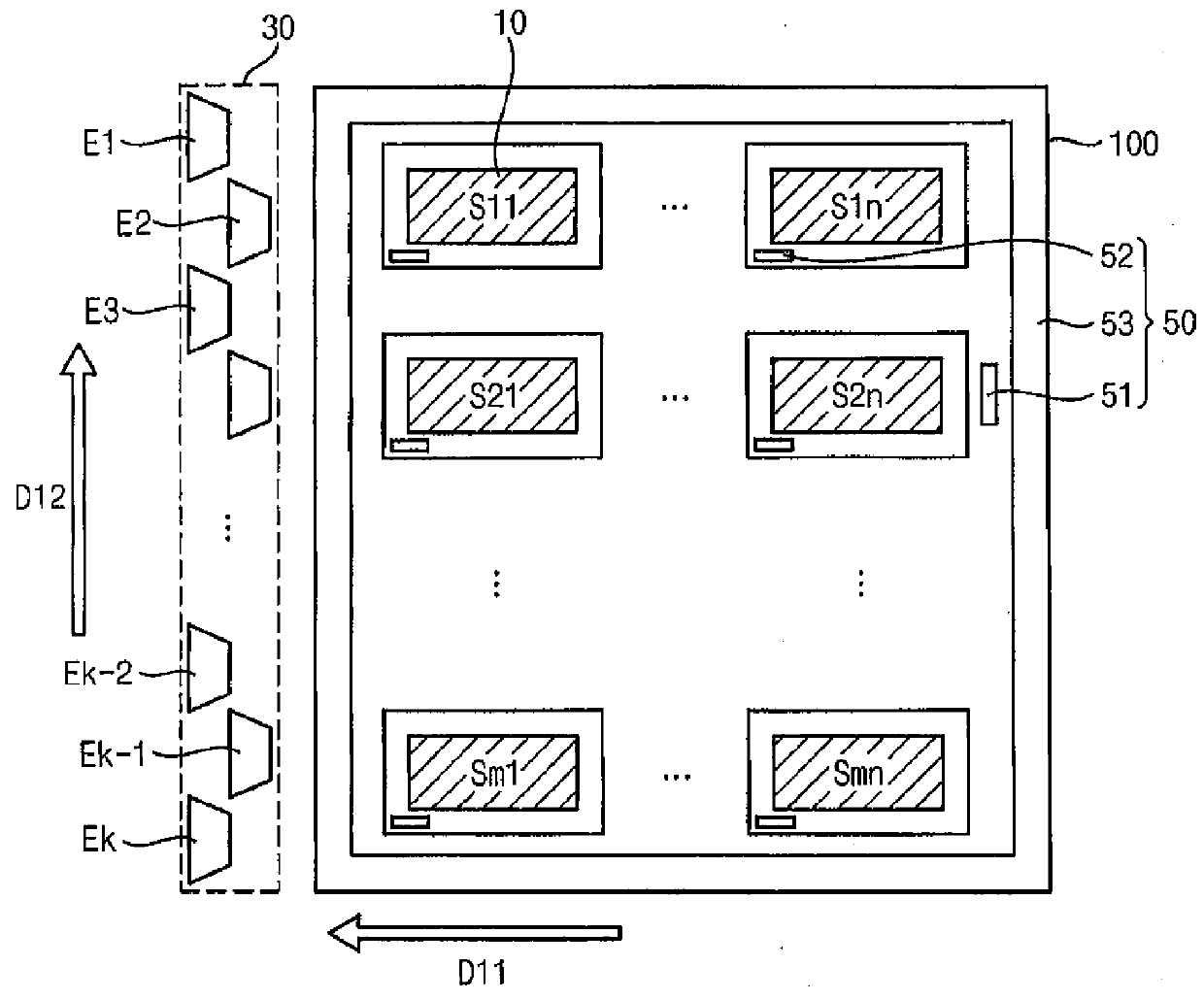
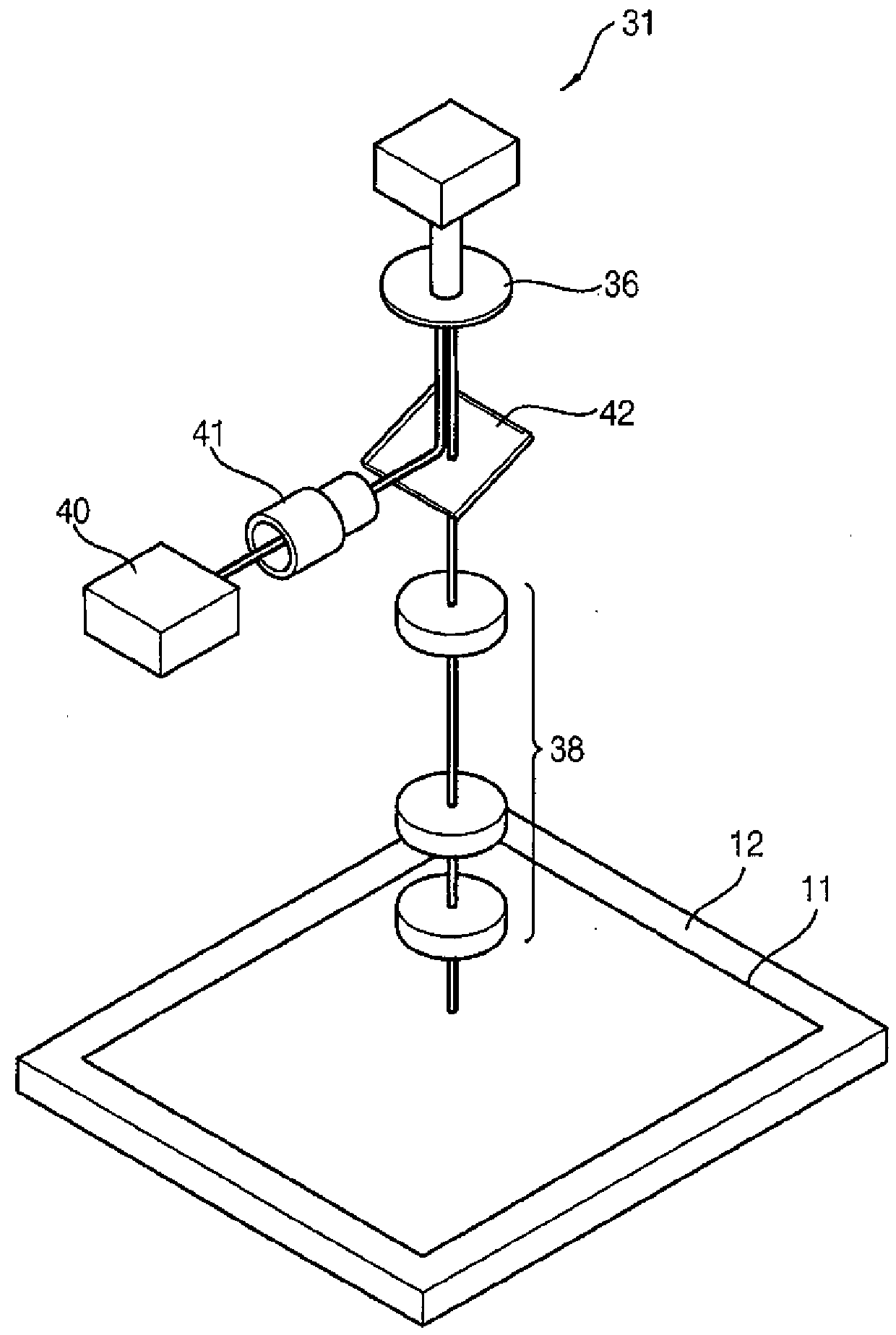
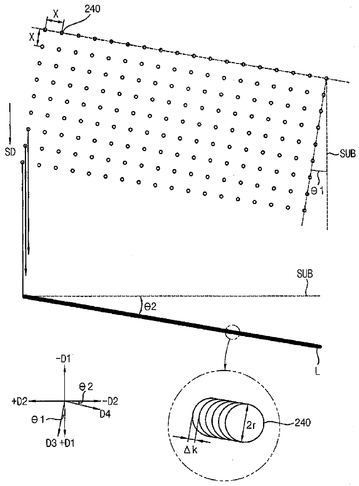
[0048]Hereinafter, the present invention will be explained in detail with reference to the accompanying drawings. In the following detailed description, only certain embodiments of the present invention are shown and described, by way of illustration. As those skilled in the art would recognize, the invention may be embodied in many different forms and should not be construed as being limited to the embodiments set forth herein. Also, in the context of the present application, when a first element is referred to as being “on” a second element, it can be directly on the second element or be indirectly on the second element with one or more intervening elements interposed therebetween. Further, in the context of the present application, when, a first element is referred to as being “coupled or connected to” a second element, it can be directly coupled or connected to the second element or be indirectly coupled or connected to the second element with one or more intervening elements in...


PUM

PropertyMeasurementUnit
angleaaaaaaaaaa
angleaaaaaaaaaa
angle θ1aaaaaaaaaa

Abstract

A maskless exposure device includes an exposure head including a digital micro-mirror device, the digital micro-mirror device being configured to scan an exposure beam to a substrate by reflecting a source beam from an exposure source; and a system control part configured to control the digital micro-mirror device by utilizing a graphic data system file. The graphic data system file includes data for a source electrode, a drain electrode and a channel portion between the source electrode and the drain electrode in a plan view. The channel portion includes a first portion extending in a direction perpendicular to a scan direction of the exposure head. A width of the first portion of the channel portion is defined to be a multiple of a pulse event generation of the exposure beam.

Description

CROSS-REFERENCE TO RELATED APPLICATION[0001]This application claims priority to and the benefit of Korean Patent Application No. 10-2014-0110922, filed on Aug. 25, 2014 in the Korean Intellectual Property Office (KIPO), the entire content of which is incorporated herein by reference.BACKGROUND[0002]1. Field[0003]Exemplary embodiments of the present inventive concept relate to a maskless exposure device, a maskless exposure method and a display substrate manufactured by the maskless exposure device and / or the maskless exposure method.[0004]2. Description of the Related Art[0005]Generally, to form a metal pattern including a thin film transistor (“TFT”), which is a switching element of a display substrate and signal lines, a metal layer and a photoresist layer are sequentially formed, and a mask corresponding to the metal pattern is disposed on the photoresist layer.[0006]Then, a light is irradiated to an upper surface of the mask so that the photoresist layer is exposed and developed...

Claims


Application Information

Patent Timeline
Patent Type & Authority Applications(United States)
IPC IPC(8): G03F7/20H01L27/12H01L29/786
CPCG03F7/702H01L29/78693H01L27/1225H01L27/124H01L29/78663H01L27/1222H01L29/78696G03F7/70291G03F7/70508H01L27/1285H01L29/41733
Inventor LEE, SANG-HYUNKIM, HYUN-SEOKHEO, JUNG-CHULLEE, HI-KUKYUN, SANG-HYUNLEE, KI-BEOMKIM, CHANG-HOONPARK, JUNG-INSEO, KAB-JONGSIM, JUN-HOCHANG, JAE-HYUK
Owner SAMSUNG DISPLAY CO LTD
Why Eureka
Try Eureka