Method for Focusing Electron Beam in Electron Column

a technology of electron beam and electron column, which is applied in the field of focusing electron beam in the electron column, can solve the problems of difficult to use it in the electron beam lithography, difficult to reduce the diameter of the probe beam, and critical affecting the electron beam energy of the electron column, etc., to achieve the effect of improving resolution, small spot size and increasing working distan

Inactive Publication Date: 2009-08-13
CEBT
View PDF7 Cites 7 Cited by
  • Summary
  • Abstract
  • Description
  • Claims
  • Application Information

AI Technical Summary

Benefits of technology

[0024]When the focusing control method for an electron column according to the present invention is used, an electron beam that reaches to the specimen has a small spot size, so that there are advantages in that resolution can be improved in the case where the electron column is used for an electron microscope, and in that the working distance can also be increased. Furthermore, in an electron beam lithography, the width of a pattern can be further reduced and the depth of the pattern can be increased, therefore improved patterning can be performed.
[0025]When the focusing control method for an electron column according to the present invention is used, desired electron beam energy can be achieved without applying an additional high voltage to the electron emitter, so that damage to the tip of the electron emitter does not occur and the cost of maintaining ultrahigh vacuum is also reduced.

Problems solved by technology

That is, the difference between the voltage applied to the electron emitter and the voltage applied to the last electrode layer of the lens (the last electrode layer of the focusing lens) critically affects the electron beam energy of the electron column.
Since such a deflection-aberration is relatively unimportant compared to other aberrations, it is frequently excluded from calculations.
However, there are limitations in the ability to reduce the diameter of the probe beam due to various factors.
The chromatic aberration and the spherical aberration are generated by each lens, which is one major problem that must be solved to improve the characteristics of the probe beam.
However, the electron beam that reaches the specimen has a large spot size, so that the method is disadvantageous in that it is difficult to use it to perform a high resolution patterning process, or to use it in an electron beam lithography.

Method used


Image

  • Method for Focusing Electron Beam in Electron Column
  • Method for Focusing Electron Beam in Electron Column
  • Method for Focusing Electron Beam in Electron Column

Examples


Embodiment Construction

[0030]An embodiment of the present invention is described with reference to the accompanying drawings below.

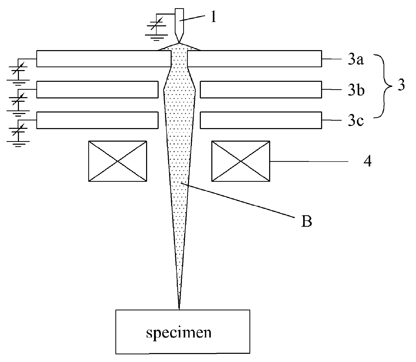
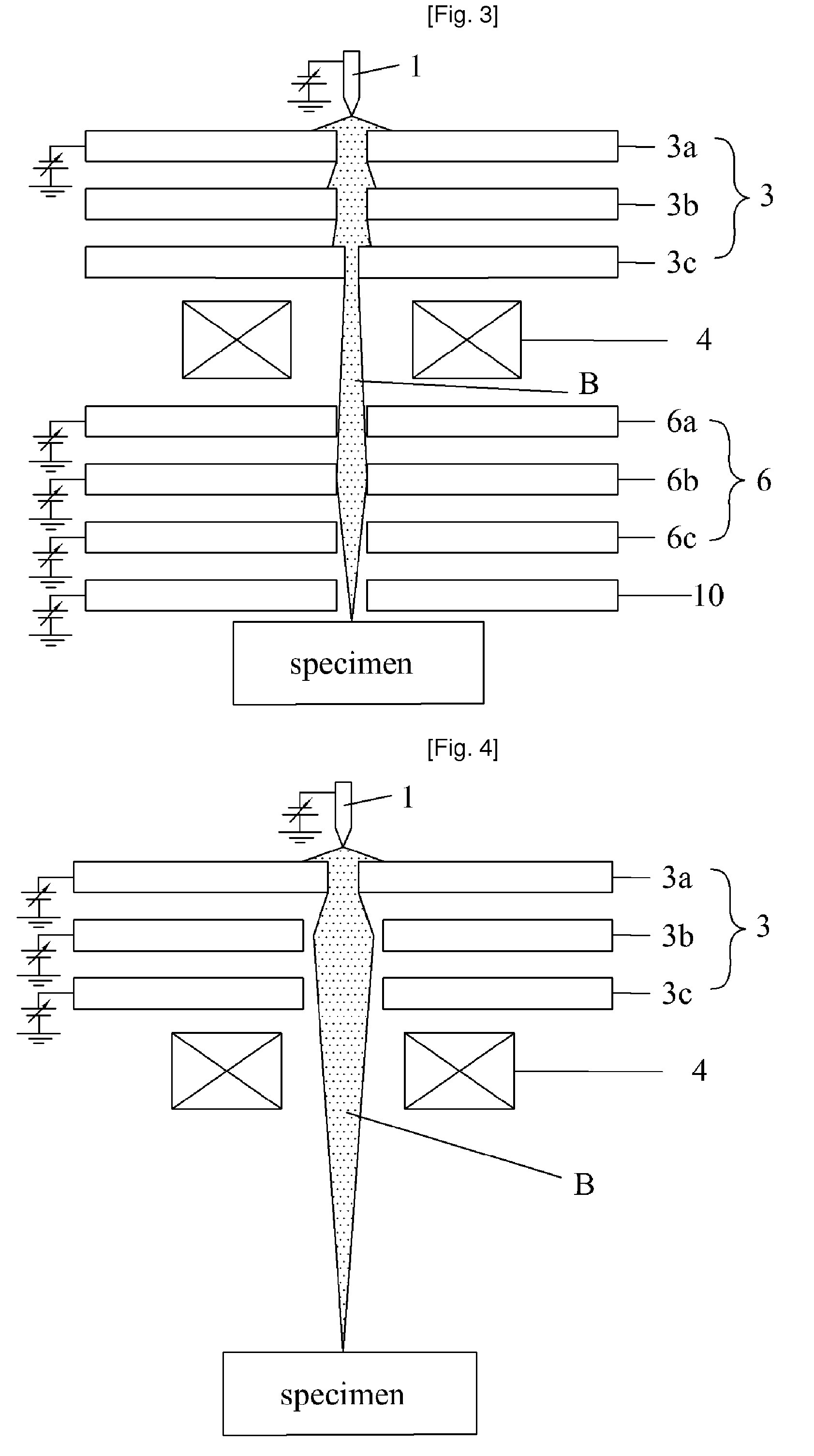
[0031]FIG. 3 shows an embodiment to which a method for focusing an electron beam according to the present invention is applied, in which the electron beam is controlled in the typical electron column.

[0032]When a negative voltage ranging from several hundreds of eV to several KeV is applied to an electron emitter 1, and a voltage higher than that applied to the electron emitter is applied to the extractor electrode layer 3a of a source lens 3, electrons are emitted from the electron emitter and move to the extractor electrode layer to which the high voltage is applied. For example, when a voltage of −500 eV is applied to the electron emitter 1, electrons are emitted from the electron emitter 1 in such a way that a voltage (for example, −200 eV or +200 eV) higher than that applied to the electron emitter is applied to the extractor electrode layer 3a. The emitted electrons are ...


PUM


Abstract

The present invention relates to a method for improving focusing in an electron column that generates an electron beam. The method for controlling the focusing of an electron beam in according to the present invention reduces the spot size of the electron beam when the electron beam reaches a specimen, so that resolution can be increased and the line width of a pattern in a semiconductor lithography process can be reduced, with the result that the performance of the electron can be improved.

Description

TECHNICAL FIELD[0001]The present invention relates, in general, to a method for focusing an electron beam in an electron column that generates the electron beam and, more particularly, to a method for increasing the energy of an electron beam while focusing the electron beam in the electron column, so that the spot size of the focused electron beam is further reduced, with the result that precise focusing can be achieved and the energy of the electron beam can be adjusted.BACKGROUND ART[0002]FIG. 1 shows the structure of a conventional microcolumn, a miniaturized electron column. The electron column includes an electron emitter 1 for emitting electrons, a source lens 3 formed of three electrode layers, that is, an extractor electrode layer 3a, an accelerator electrode layer 3b and a limiting aperture electrode layer 3c, and configured to cause electrons to be emitted from the electron emitter and to effectively form the emitted electrons into an beam, a deflector 4 for deflecting th...

Claims


Application Information

Patent Timeline
Patent Type & Authority Applications(United States)
IPC IPC(8): H01J3/14
CPCB82Y10/00H01J37/3174H01J37/12B82Y40/00H01J37/147
Inventor KIM, HO SEOBAHN, SEUNG JOONKIM, DAE WOOKKIM, YOUNG CHUL
Owner CEBT
Why Eureka
Try Eureka