Optical coupling device and process for fabrication thereof

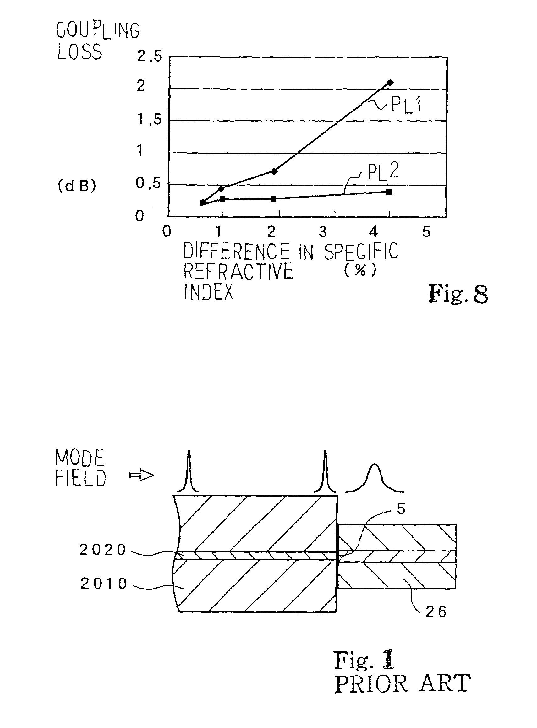
a coupling device and optical technology, applied in the field of optical devices, can solve the problems of large coupling loss, narrow spot size, increased coupling loss, etc., and achieve the effect of reducing spot size and increasing coupling loss

Inactive Publication Date: 2006-08-29
NEC CORP
View PDF13 Cites 17 Cited by
  • Summary
  • Abstract
  • Description
  • Claims
  • Application Information

AI Technical Summary

Benefits of technology

[0022]It is therefore an important object of the present invention to provide an optical coupling device, which is compact without increase of the coupling loss. Even a proximity wave-guide interference device is incorporated in the optical coupling device, the optical wave-guide device is not enlarged. A built-in spot size converter of the optical coupling device can reduce the spot size.

Problems solved by technology

One of the problems is increase of the coupling loss. FIG. 1 shows a typical example of the optical wave-guide device, and the prior art optical wave-guide device includes a wave-guide constituted by clad layers 2010 and a core layer 2020.
This results in a narrow spot size.
This results in a large coupling loss.
Thus, there is the tradeoff between the device size and the coupling loss.
This results in a large coupling loss between the wave-guide and the thin film element 2350 or between the wave-guide and the wave-guide.
Although the large difference in specific refractive index makes the prior art optical wave-guide device scaled down, the prior art optical wave-guide device is not commercially available for the optical module forming a part of the optical communication system, because the coupling loss is large.
However, the divergent spot size converters are not effective against the reduction in coupling loss in a wave-guide having the difference in specific refractive index greater than 1%.
However, the excess loss is not ignoreable due to the misalignment of the optical axes.
Although the convergent spot size converter can reduce the coupling loss rather than the divergent spot size converter, the convergent spot size converter can not satisfy the users.
However, a problem is encountered in the prior art optical wave-guide device with built-in convergent spot size converter in that the coupling loss is rather increased when the width is reduced beyond a limit.
The prior art convergent spot size converter can not achieve the low coupling loss requested by the users.
A problem inherent in the prior art fabrication process for the convergent spot size converter is a low production yield.
However, it is difficult to form such a narrow spot size converter at a high production yield.
On the other hand, the following problems are encountered in the prior art input-and- output optical wave-guide device.
First, the complicated assembling work is required for the prior art input-and- output optical wave-guide device.
This means that the alignment work is hard.
Another problem is the volume of the resultant device.
The prior art input-and-output optical wave-guide device is added to the prior art planar lightwave circuit device so that the resultant device is bulky.
Yet another problem is the limitative usage.
This means that the prior art input-and-output optical waveguide is hardly built in the prior art planar lightwave circuit device.
However, there is not a spot size converter for reducing the spot size.
Another problem due to a large difference in specific refractive index is elongation of the wave-guide.
In case where the wave-guide with a large difference in specific refractive index is formed in an optical interference circuit having proximity wave-guides such as a directional optical coupler, the wave-guide with a large difference in specific refractive index is prolonged, and, accordingly, the optical device is bulky.

Method used


Image

  • Optical coupling device and process for fabrication thereof
  • Optical coupling device and process for fabrication thereof
  • Optical coupling device and process for fabrication thereof

Examples


first embodiment

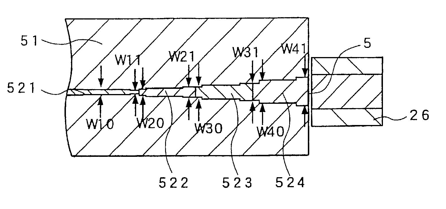
[0062]Referring to FIG. 5A of the drawings, an optical coupling device embodying the present invention is formed with the first optical wave-guides 11, second optical wave-guide 12, . . . (n−1)th optical wave-guide 13 and nth optical waveguide 14, and has an end surface 5. The optical coupling device is cut off along a certain horizontal cross-section so that the FIG. 5A is a plan view showing the certain horizontal cross-section. The nth optical wave-guide is exposed to the end surface 5 so that the output light is radiated from then nth optical wave-guide on the end surface 5. In this instance, the core layers of the first optical wave-guide 11 to then nth optical wave-guide 14 are equal in width to one another. However, the core layers may vary the width depending upon the specific refractive index thereof.

[0063]The first optical wave-guide 111 has the first clad layer 111 and the first core layer 112, the second optical wave-guide 12 has the second clad layer 121 and the second ...

second embodiment

Samples of Second Embodiment

[0097]FIG. 17A shows a sample of the optical coupling device implementing the second embodiment. The cross section was in parallel to the major surface of the substrate so that FIG. 17A shows the cross section. The sample is hereinbelow referred to as “first sample”. The optical coupling device had an optical wave-guide consisting of four wave-guides 71, 72, 73 and 74, and the wave-guide 74 was coupled to a semiconductor optical element 76. The semiconductor element 76 served as a semiconductor spot size converting optical amplification element. The distance between the end surface 5 and the semiconductor optical element 76 was 5 microns.

[0098]The substrate was made of silicon. The lower and upper clad layer 711 / 721 / 731 / 741 were made of GPSG, and the core layers 712 / 722 / 732 / 742 were also made of GPSG. The lower clad layers, core layers and upper clad layers were deposited on the major surface of the substrate by using the atmospheric pressure chemical vap...

third embodiment

[0106]Turning to FIG. 19 of the drawings, an optical coupling device embodying the present invention is fabricated on a substrate, and includes a directional optical coupler. The directional optical coupler is implemented by an optical wave-guide, which has a clad layer 1010 and core layers 1021 / 1022. The core layers 1021 and 1022 are hereinafter referred to as “first core layer” and “second core layer”, respectively.

[0107]The first core layer 1021 is optically coupled to the second core layer 1022, and the second core layer 1022 forms a proximity wave-guide interference circuit together with a second core layer of another optical wave-guide arranged in parallel to the optical wave-guide 1010 / 1021 / 1022.

[0108]The present inventor fabricated a sample of the optical coupling device implementing the third embodiment. The sample had the first core layer 1021 made of SiON, the refractive index of which was 1.480. The first core layer 1021 was 2.5 microns in both width and thickness. The s...


PUM


Abstract

An optical coupling device has an optical wave-guide varied in difference in specific refractive index between a clad layer and a core layer, and the optical wave-guide serves as a convergent/divergent spot size converter; since reduction in cross section of the core layer is not required for the convergent/divergent spot size converter so that the optical coupling device is produced at a high production yield.

Description

FIELD OF THE INVENTION[0001]This invention relates to an optical device available for the optical communication and, more particularly, to an optical coupling device having a spot size converter with plural optical wave-guides and a process for fabricating the optical coupling device.DESCRIPTION OF THE RELATED ART[0002]The internet has been spreading worldwide, and the optical communication systems are being commercialized. A 10 giga-bit / second system is capable of handing more than a hundred twenty thousand channels. The amount of information transferred through the channels makes great strides with the wavelength division multiplexing technologies. Optical wave-guide devices called as planar lightwave circuits are indispensable elements for the large scale communication systems. The planar lightwave circuits are usually abbreviated as PLCs.[0003]Array wave-guide arrays, which achieve the optical multiplex / optical de-multiplex in the wavelength division multiplexing systems, and tr...

Claims


Application Information

Patent Timeline
Patent Type & Authority Patents(United States)
IPC IPC(8): G02B6/26G02B6/12G02B6/122G02B6/13G02B6/30
CPCG02B6/1228G02B6/305G02B2006/12147G02B2006/12116
Inventor SHIMODA, TSUYOSHI
Owner NEC CORP
Why Eureka
Try Eureka