Organic electroluminescent device and electronic apparatus

Active Publication Date: 2016-03-03
SEIKO EPSON CORP
View PDF2 Cites 9 Cited by
  • Summary
  • Abstract
  • Description
  • Claims
  • Application Information

AI Technical Summary

Benefits of technology

[0006]An advantage of some aspects of the invention is provided to an organic electroluminescent device and

Problems solved by technology

However, when a capacitive electrode is formed on a layer on which a scanning line, a gate electrode, or the like is formed as in JP-A-2007-226184, it is necessary to form

Method used


Image

  • Organic electroluminescent device and electronic apparatus
  • Organic electroluminescent device and electronic apparatus
  • Organic electroluminescent device and electronic apparatus

Examples


first embodiment

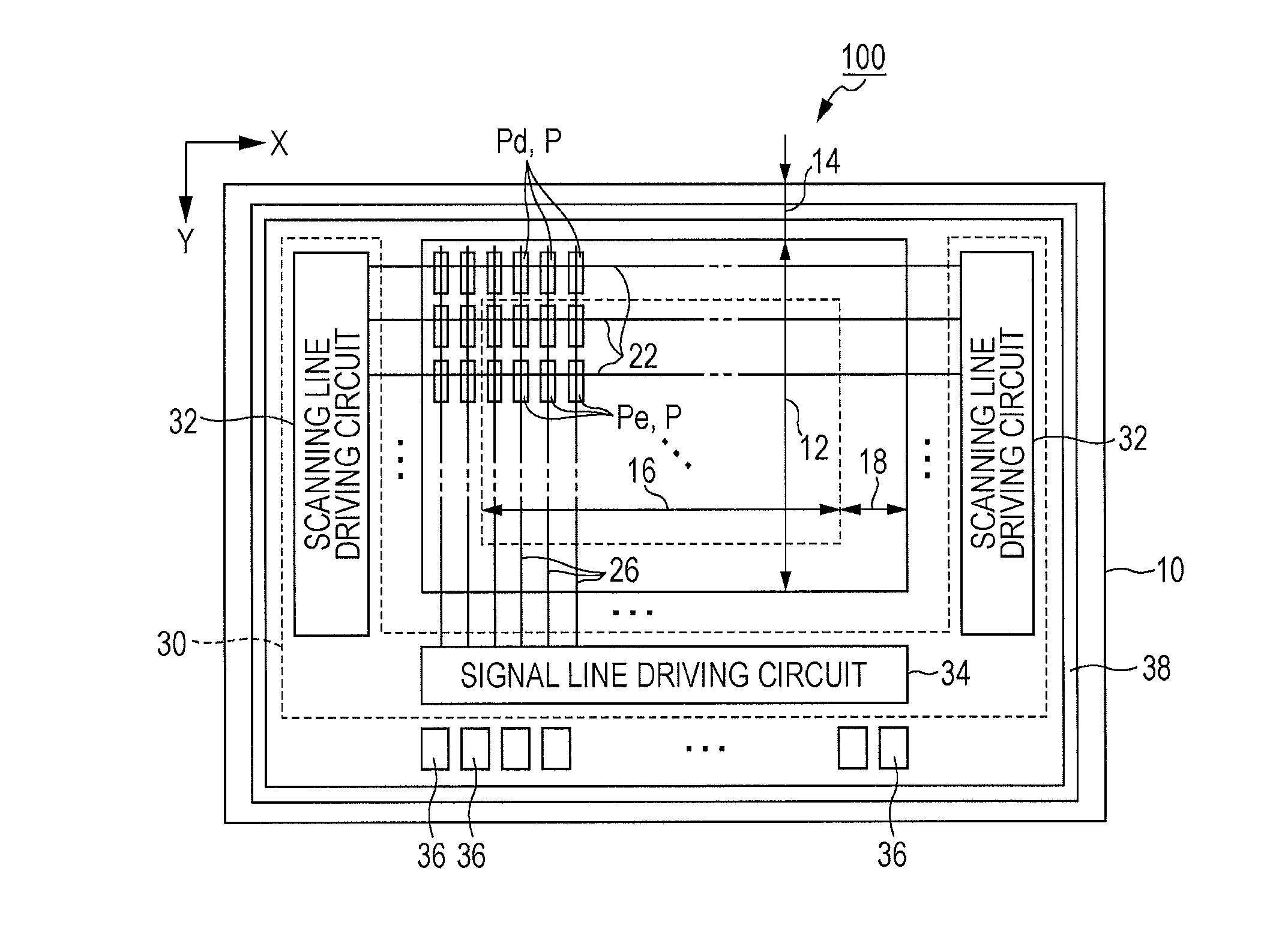
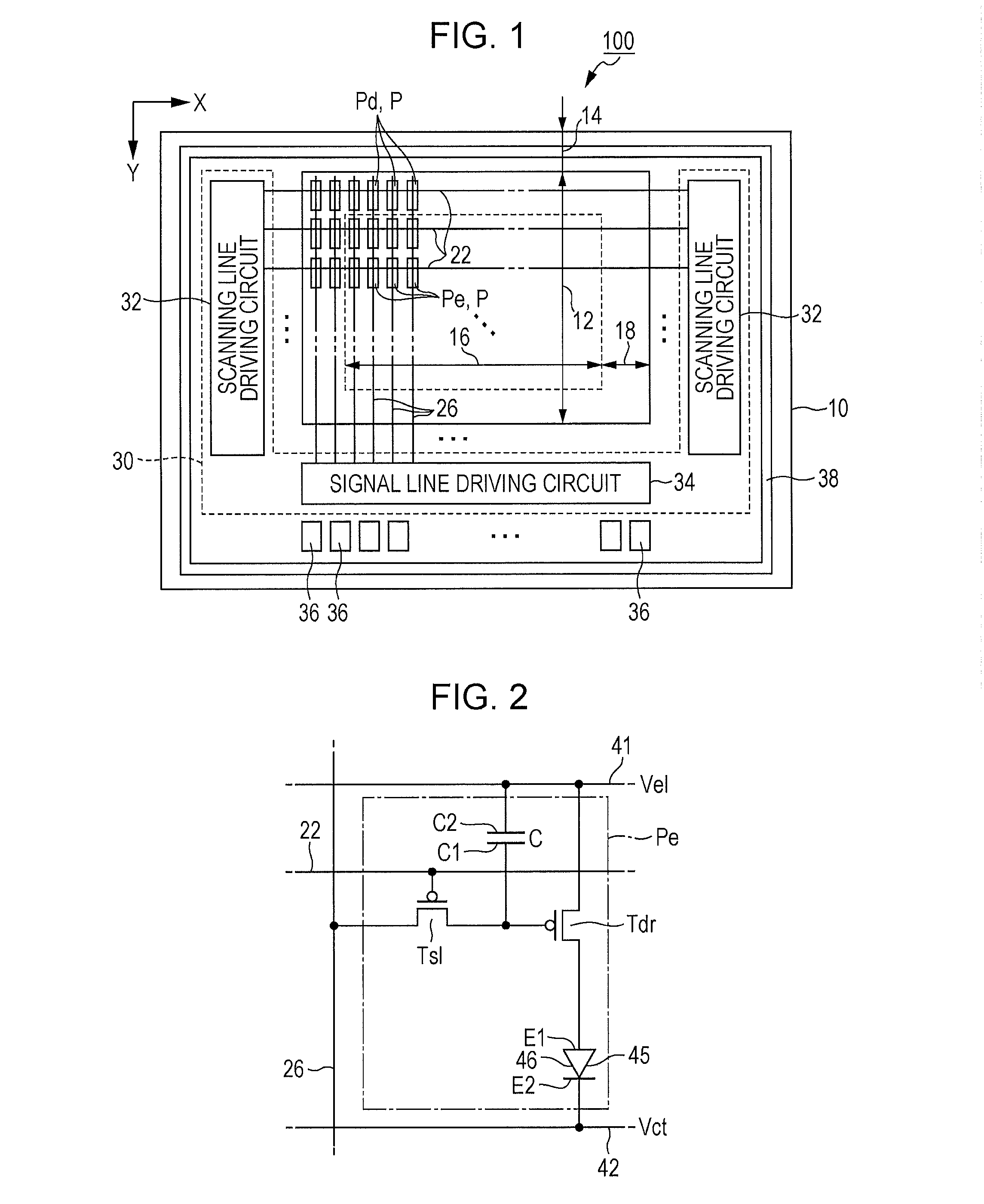
[0090]FIG. 1 is a plan view of an organic electroluminescent device 100 according to a first embodiment of the invention. The organic electroluminescent device 100 of the first embodiment is an organic EL device in which a light emitting device using an organic EL material has been formed on a surface of a substrate 10. The substrate 10 is a plate-shaped member (semiconductor substrate) formed of a semiconductor material such as silicon, and is used as a substrate (base) on which a plurality of light emitting elements are formed. As illustrated in FIG. 1, the surface of the substrate 10 is divided into a first area 12 and a second area 14. The first area 12 is a rectangular area, and the second area 14 is a rectangular frame-shaped area that surrounds the first area 12.

[0091]In the first area 12, a plurality of scanning lines 22 extending in an X direction, and a plurality of the signal lines 26 extending in a Y direction crossing the X direction are formed. A pixel P (Pd or Pe) is ...

second embodiment

[0153]A second embodiment of the invention will be described. Further, in each form to be illustrated below, elements having the same operation or function as in the first embodiment are denoted with signs referred to in the description of the first embodiment, and each detailed description will be appropriately omitted.

[0154]FIG. 18 is a circuit diagram of each display pixel Pe in this embodiment. As illustrated in FIG. 18, the display pixel Pe in this embodiment includes an emission control transistor Tel and a compensation transistor Tcmp, in addition to a light emitting element 45, a driving transistor Tdr, a selection transistor Tsl, and a capacitive element C. Further, in this embodiment, although the transistors T (Tdr, Tel, Tsl, and Tcmp) of the display pixel Pe are a P-channel type, an N-channel type transistor can also be used. A circuit of the display pixel Pe in this embodiment can be driven using any one of a so-called coupling driving scheme and a so-called current pro...

third embodiment

[0193]A third embodiment of the invention will be described. Further, in each form to be illustrated below, elements having the same operation or function as in the first embodiment and the second embodiment are denoted with the signs referred to in the description of the first and second embodiments, and each detailed description will be appropriately omitted.

[0194]A circuit of each display pixel Pe of the third embodiment is the same as the circuit of the second embodiment, and includes a compensation transistor Tcmp and an emission control transistor Tel. A specific structure of the organic electroluminescent device 100 according to the third embodiment is substantially the same structure as the specific structure of the organic electroluminescent device 100 of the second embodiment. Hereinafter, only a difference will be described for simplification.

[0195]FIG. 32 is a sectional view of the organic electroluminescent device 100, and FIGS. 33 to 40 are plan views illustrating a st...


PUM


Abstract

An organic electroluminescent device includes a first transistor, an organic electroluminescent element that emits light with luminance corresponding to magnitude of a current supplied via the first transistor, and a capacitive element. The capacitive element includes a first electrode connected to a gate of the first transistor, a second electrode, and a dielectric film provided between the first electrode and the second electrode. The first electrode is formed on the same layer as the second electrode, and is arranged in a position away from the second electrode with the dielectric film interposed therebetween.

Description

BACKGROUND[0001]1. Technical Field[0002]The present invention relates to an organic electroluminescent (hereinafter, also referred to as an organic EL) device using a luminescent material of an organic electroluminescent material.[0003]2. Related Art[0004]For example, a light emitting device in which light emitting elements using an organic EL material are arranged in a plane shape on a substrate has been conventionally proposed as a display device for various electronic apparatuses. JP-A-2007-226184 discloses a technology for forming a capacitive electrode constituting a capacitive element on a layer on which a scanning line, a gate electrode or the like is formed.[0005]However, when a capacitive electrode is formed on a layer on which a scanning line, a gate electrode, or the like is formed as in JP-A-2007-226184, it is necessary to form the capacitive electrode while avoiding a control line such as the scanning line, or the gate electrode, and it is difficult to secure capacitanc...

Claims


Application Information

Patent Timeline
IPC IPC(8): G09G3/30
CPCG09G3/30G09G2330/00G09G2300/0426G09G2330/028G09G3/3233G09G2300/0842G09G2310/0262H10K59/1216H10K59/124
Inventor OTA, HITOSHINOZAWA, RYOICHI
Owner SEIKO EPSON CORP
Why Eureka
Try Eureka