Organic light emitting diode display and manufacturing method thereof

Inactive Publication Date: 2016-03-03
SAMSUNG DISPLAY CO LTD
View PDF2 Cites 8 Cited by
  • Summary
  • Abstract
  • Description
  • Claims
  • Application Information

AI Technical Summary

Benefits of technology

[0033]In addition, subsequently, the data line partially exposed by the cover separator is etched to be separated into

Problems solved by technology

In this case, a tact time of the OS test increases and equipment is neces

Method used


Image

  • Organic light emitting diode display and manufacturing method thereof
  • Organic light emitting diode display and manufacturing method thereof
  • Organic light emitting diode display and manufacturing method thereof

Examples


Example

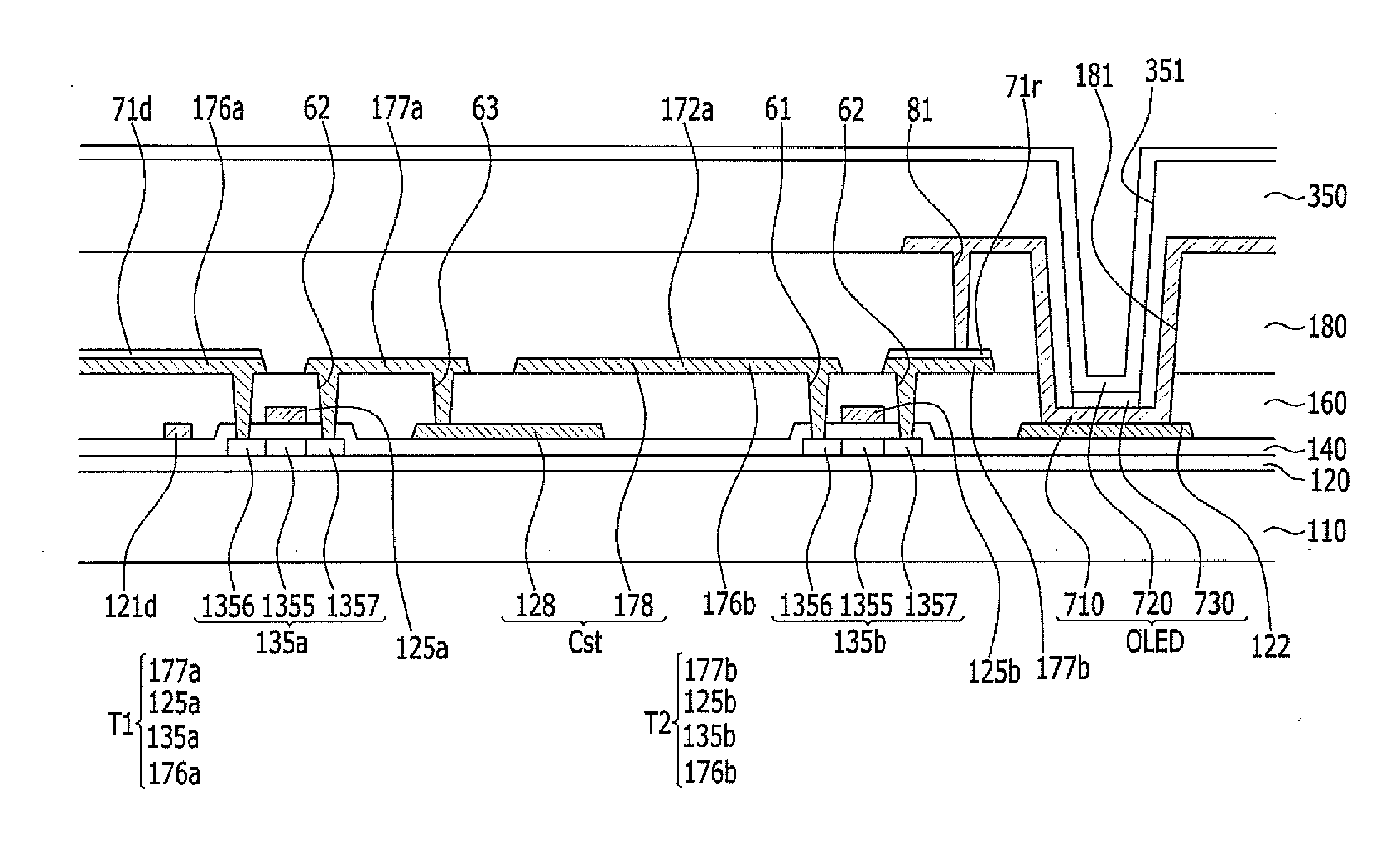
[0055]The present disclosure will be described more fully hereinafter with reference to the accompanying drawings, in which exemplary embodiments of the invention are shown.

[0056]As those skilled in the art would realize, the described embodiments may be modified in various different ways, all without departing from the spirit or scope of the present disclosure.

[0057]Parts that are irrelevant to the description will be omitted to clearly describe the present disclosure, and the same or similar constituent elements will be designated by the same reference numerals throughout the specification.

[0058]Further, in the drawings, size and thickness of each element are arbitrarily illustrated for ease of description, and the present disclosure is not necessarily limited to those illustrated in the drawings.

[0059]In the drawings, the thickness of layers, films, panels, regions, etc., are exaggerated for clarity.

[0060]In the drawings, for ease of description, the thicknesses of some layers an...


PUM


Abstract

An organic light emitting diode (OLED) display includes an OLED display panel having a substrate; a plurality of scan lines formed on the substrate; a plurality of data lines crossing the plurality of scan lines; cover lines covering the data lines; a plurality of switching elements coupled to the plurality of scan lines and the plurality of data lines; and a plurality of organic light emitting diodes coupled to the plurality of switching elements; and upper and lower data drivers respectively located at upper and lower parts of the OLED display panel, wherein the data lines include an upper data line and a lower data line that are separated from each other, and the cover lines include upper and lower cover lines that are separated from each other.

Description

CROSS-REFERENCE TO RELATED APPLICATION[0001]This application claims priority to and the benefit of Korean Patent Application No. 10-2014-0116356 filed in the Korean Intellectual Property Office on Sep. 2, 2014, the entire contents of which are incorporated herein by reference.BACKGROUND[0002]1. Field[0003]The present disclosure relates to an organic light emitting diode (OLED) display and a manufacturing method thereof.[0004]2. Description of the Related Art[0005]An organic light emitting diode (OLED) display includes two electrodes and an organic emission layer located therebetween, electrons injected from one electrode (e.g., a cathode) and holes injected from the other electrode (e.g., an anode) are combined in the organic emission layer to generate excitons, and the excitons release energy to emit light.[0006]The OLED display includes a plurality of pixels including an OLED consisting of the anode, the cathode, and the organic emission layer, and a plurality of thin film transis...

Claims


Application Information

Patent Timeline
IPC IPC(8): H01L51/00H01L27/32
CPCH01L51/0031H01L51/56H01L27/3258H01L27/3276H10K59/352H10K59/123H10K59/124H10K59/131H10K71/70
Inventor PARK, JONG-HYUNYOU, CHUN, GI
Owner SAMSUNG DISPLAY CO LTD
Why Eureka
Try Eureka