Integrated chip package with optical interface

a chip and integrated technology, applied in the field of integrated chip packages, can solve the problems of high bandwidth, low power, reliability and low cost, and the inability of existing interconnection technologies to provide suitable communication characteristics, and achieve the bandwidth, size, power requirements of input/output interfaces for future chips, and the difficulty of scaling these photonic components to meet the bandwidth, power requirements, and power requirements of future chips

Active Publication Date: 2016-03-24
ORACLE INT CORP
View PDF3 Cites 55 Cited by
  • Summary
  • Abstract
  • Description
  • Claims
  • Application Information

AI Technical Summary

Problems solved by technology

As integrated-circuit (IC) technology continues to scale to smaller critical dimensions, it is increasingly difficult for existing interconnection technologies to provide suitable communication characteristics, such as: high bandwidth, low power, reliability and low cost.
However, while photonic technologies based on vertical cavity surface-emitting lasers (VCSELs) and optical fibers are typically a convenient and cost-effective solution to communicate modest amounts of data in certain parts of systems (such as between racks and, in certain cases, between boards within a rack), it is often difficult to scale these photonic components to meet the bandwidth, size, and power requirements of input / output (I / O) interfaces for future chips.
However, it can be difficult to integrate optical integrated circuits with conventional integrated circuits in existing chip packages.
Furthermore, the communication between the integrated circuit and the optical integrated circuit may be unidirectional.

Method used


Image

  • Integrated chip package with optical interface
  • Integrated chip package with optical interface
  • Integrated chip package with optical interface

Examples


Embodiment Construction

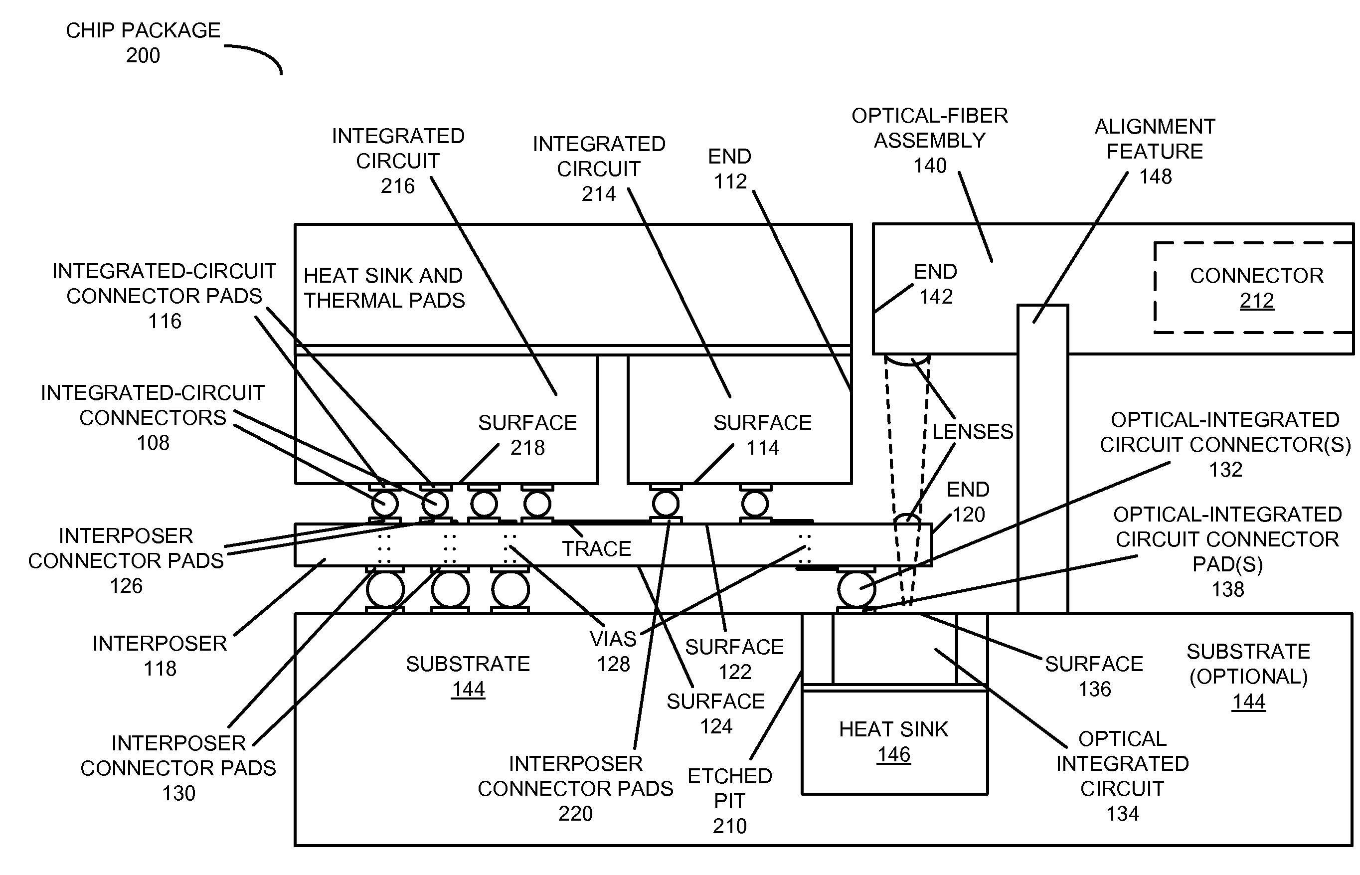
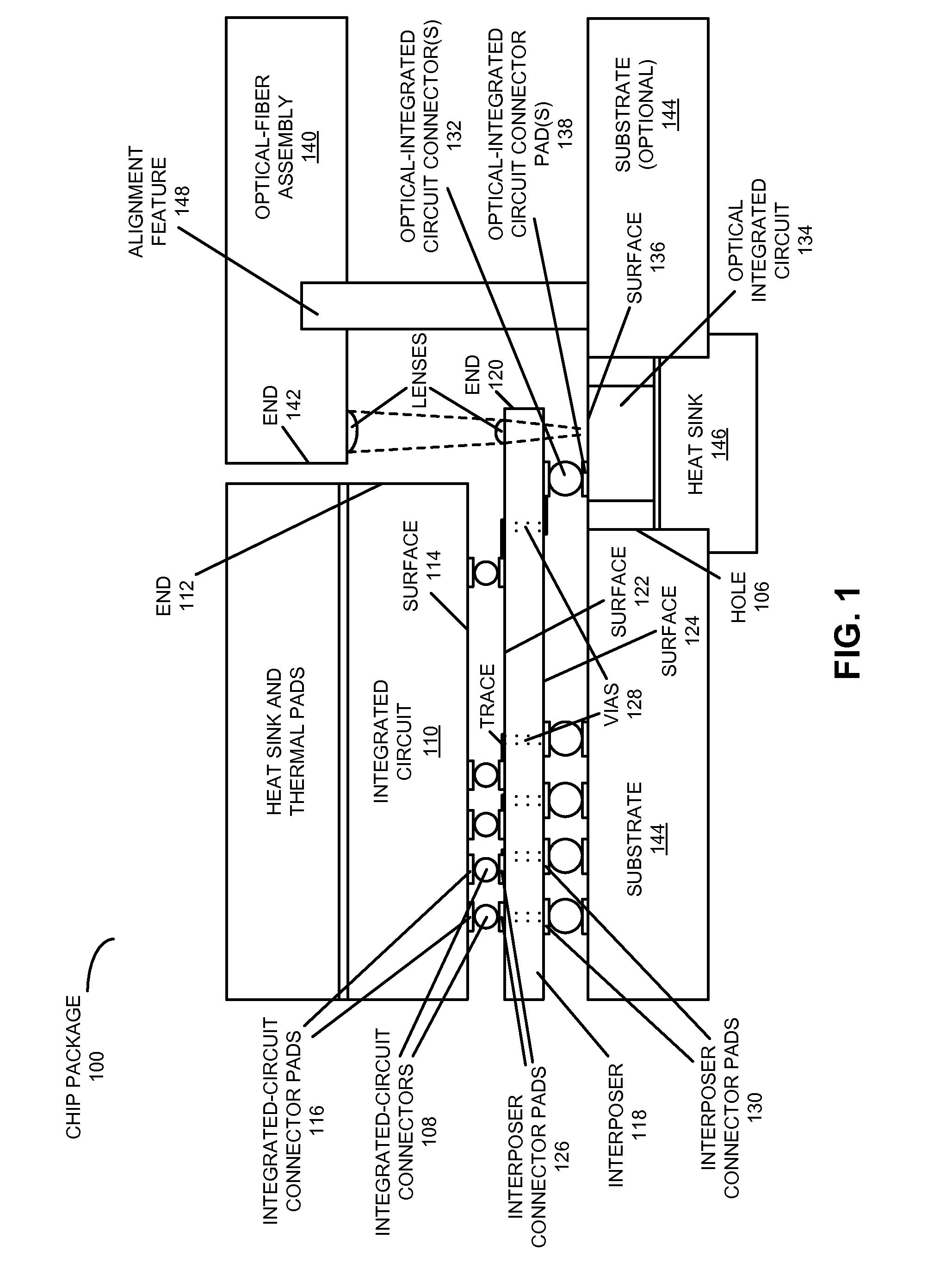
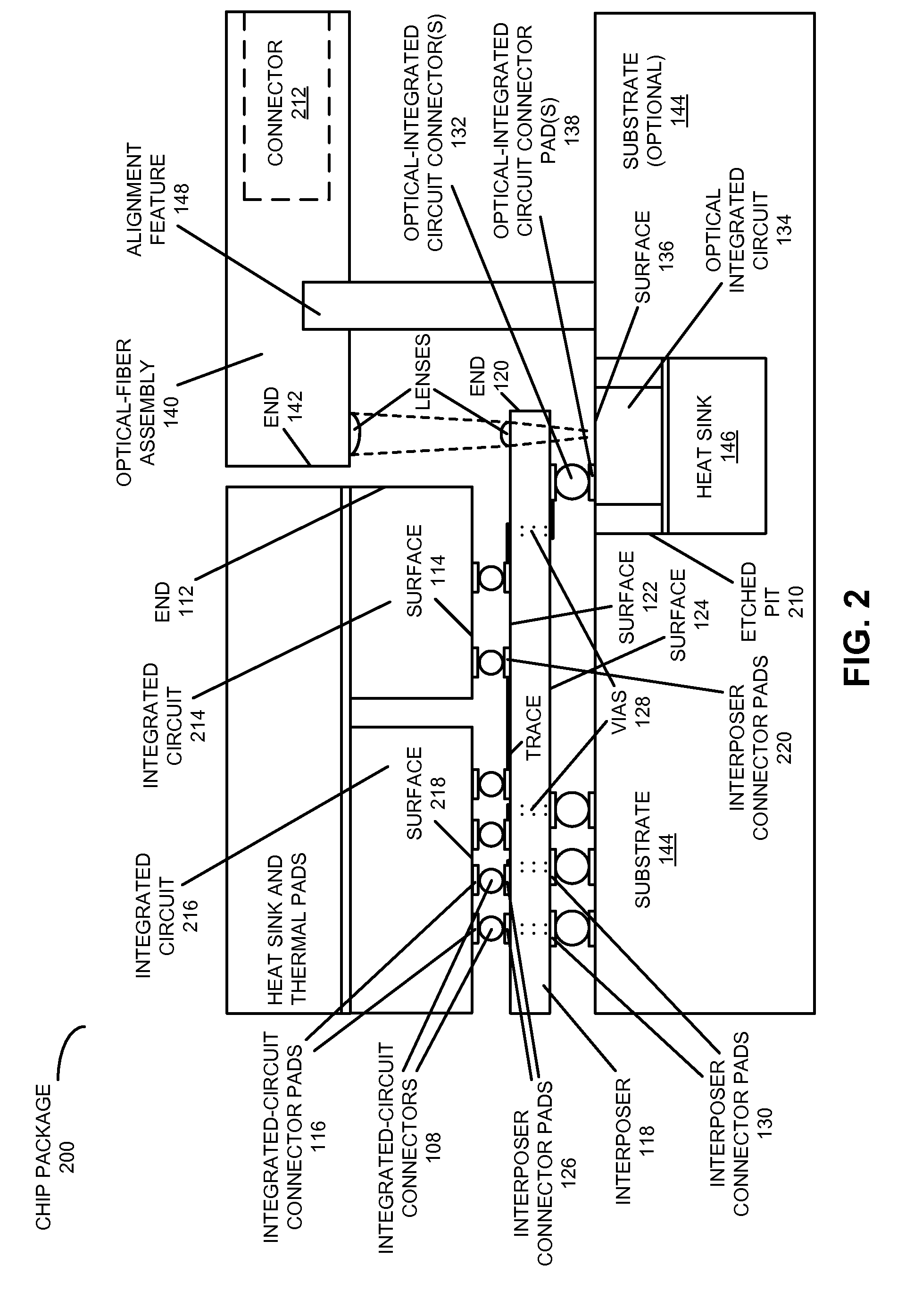
[0028]Embodiments of a chip package, a system that includes the chip package, and a technique for communicating information in the chip package are described. This chip package may include an integrated circuit and an optical integrated circuit (such as a hybrid integrated circuit) with an optical source and / or an optical receiver. The integrated circuit and the optical integrated circuit may be proximate to each other on opposite sides of an interposer in the chip package. Moreover, the integrated circuit may include a driver circuit of electrical signals for the optical source and / or a receiver circuit of electrical signals from the optical receiver. Furthermore, the optical integrated circuit may be positioned in a hole or an etch pit in a substrate, and an alignment feature may mechanically couple the substrate to an optical-fiber assembly, so that the optical-fiber assembly is positioned relative to the interposer and the optical integrated circuit. Additionally, the optical-fi...


PUM


Abstract

A chip package includes an integrated circuit and an optical integrated circuit (such as a hybrid integrated circuit) with an optical source and/or an optical receiver. The integrated circuit and the optical integrated circuit may be proximate to each other on opposite sides of an interposer in the chip package. Moreover, the integrated circuit may include a driver circuit of electrical signals for the optical source and/or a receiver circuit of electrical signals from the optical receiver. Furthermore, the optical integrated circuit may be positioned in a hole or an etch pit in a substrate, and an alignment feature may mechanically couple the substrate to an optical-fiber assembly, so that the optical-fiber assembly is positioned relative to the interposer and the optical integrated circuit. In particular, the optical-fiber assembly may partially overlap the interposer, so that optical signals are provided and/or received from the optical integrated circuit through the interposer.

Description

BACKGROUND[0001]1. Field[0002]The present disclosure generally relates to a chip package that accommodates semiconductor chips. More specifically, the present disclosure relates to a hybrid-integrated chip package that includes a substrate with adjacent payload and photonic chips, and which has one or more high-speed optical serial data interfaces.[0003]2. Related Art[0004]As integrated-circuit (IC) technology continues to scale to smaller critical dimensions, it is increasingly difficult for existing interconnection technologies to provide suitable communication characteristics, such as: high bandwidth, low power, reliability and low cost. Engineers and researchers are investigating a variety of interconnect technologies to address these problems, and to enable future high-density, high-performance systems.[0005]One interconnect technology to address these challenges, which is the subject of ongoing research, is optical communication. In principle, optical communication can be used...

Claims


Application Information

Patent Timeline
Patent Type & Authority Applications(United States)
IPC IPC(8): G02B6/42G02B6/122G02B6/43
CPCG02B6/4257G02B6/122G02B2006/12085G02B6/4202G02B6/4269G02B6/43G02B6/4204G02B6/423G02B6/428
Inventor DECKER, PATRICK, J.RAJ, KANNANHILTON-NICKEL, ALAN, T.
Owner ORACLE INT CORP
Why Eureka
Try Eureka