Optical apparatus and display apparatus provided with same
- Summary
- Abstract
- Description
- Claims
- Application Information
AI Technical Summary
Benefits of technology
Problems solved by technology
Method used
Image

Examples
embodiment 1
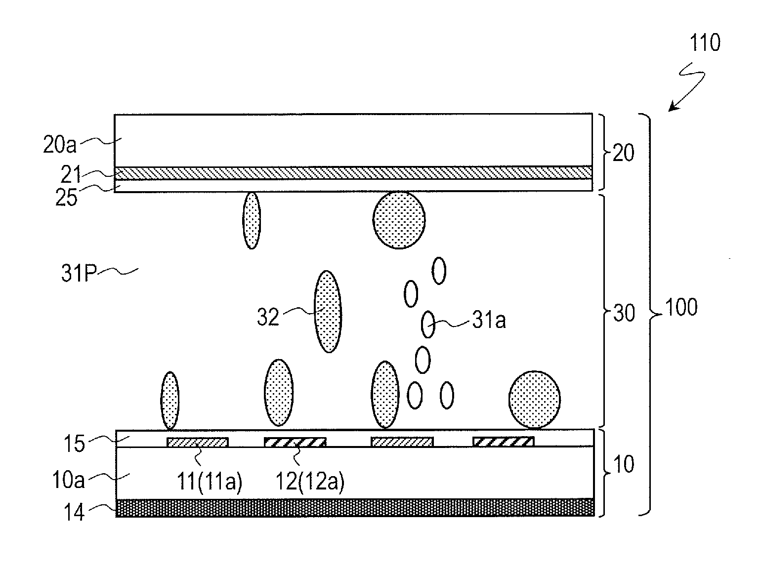
[0077]FIG. 1 shows a display device 110 according to the present embodiment. FIG. 1 is a cross-sectional view schematically showing the display device 110.
[0078]The display device 110 is a reflection type display device that can perform displaying in a reflection mode by utilizing light which is incident from the exterior (ambient light). As shown in FIG. 1, the display device 110 includes a display panel (optical device) 100, and has a plurality of pixels in a matrix array.
[0079]The display panel 100 includes a first substrate 10 and a second substrate 20 opposing each other, and an optical layer (display medium layer) 30 which is provided between the first substrate 10 and the second substrate 20. Between the first substrate 10 and the second substrate 20, the first substrate 10 that is relatively located on the rear face side may hereinafter be referred to as the “rear substrate”, whereas the second substrate 20 that is relatively located on the front face side (i.e., the viewer'...
embodiment 2
[0137]FIG. 11 shows a display device 210 according to the present embodiment. FIG. 11 is a cross-sectional view schematically showing the display device 210. Hereinafter, differences of the display device 210 of the present embodiment from the display device 110 of Embodiment 1 will be mainly described.
[0138]The display panel 100 of the display device 110 of Embodiment 1 includes a positive type liquid crystal material as the medium 31P. On the other hand, a display panel 200 of the display device 210 of the present embodiment includes a so-called negative type liquid crystal material as a medium 31N. In other words, the medium 31N is a liquid crystal material having negative dielectric anisotropy, such that the dielectric constant ∈⊥ of the liquid crystal molecules 31b along the minor axis direction is greater than the dielectric constant ∈ / / along the major axis direction.
[0139]Now, with reference also to FIG. 12 and FIG. 13, changes in the alignment direction of anisotropically-s...
embodiment 3
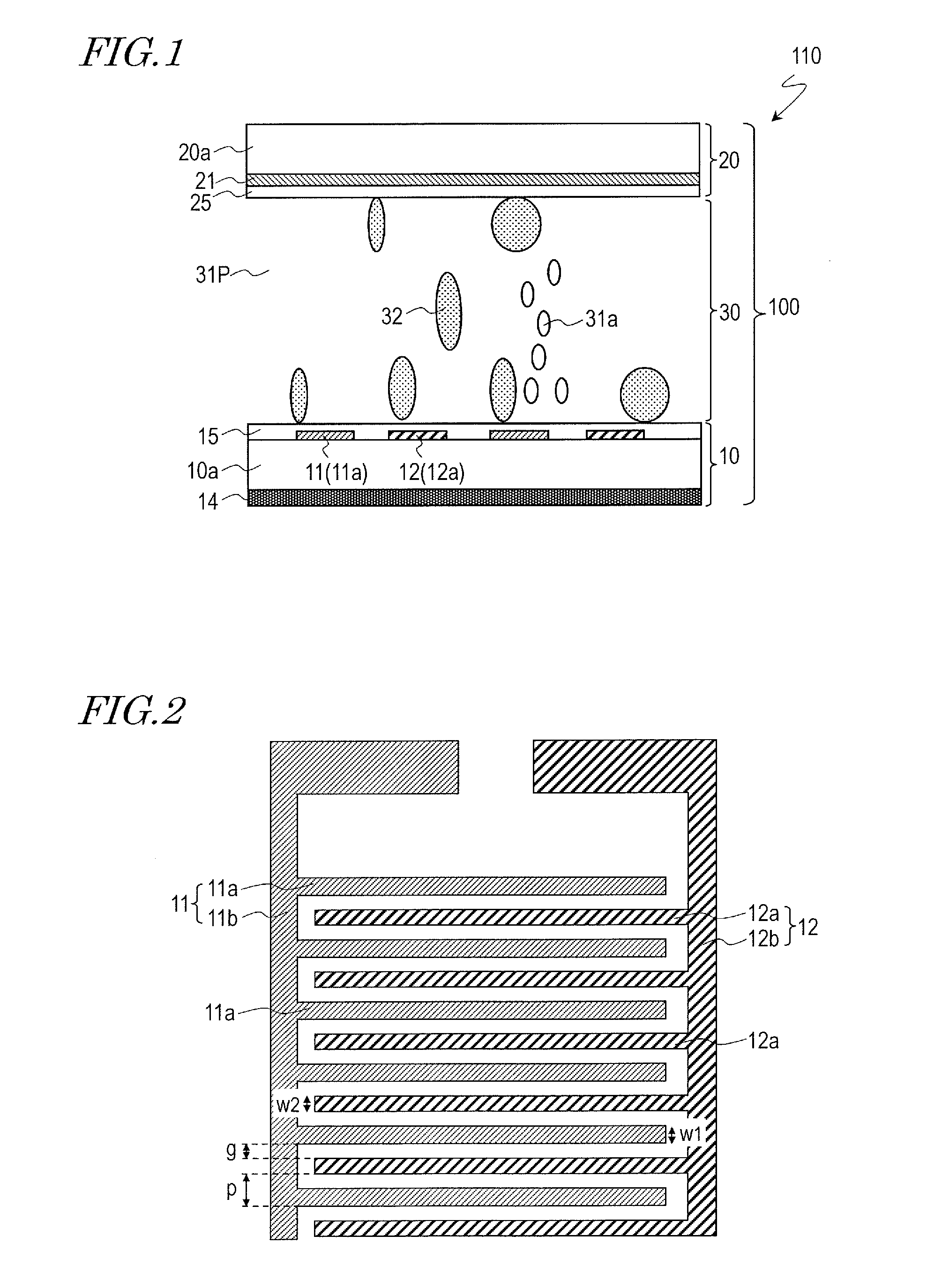
[0159]With reference to FIG. 17 to FIG. 22, a display device 310 according to the present embodiment will be described. FIG. 17 is a plan view schematically showing the entire display device 310. FIG. 18 is a plan view schematically showing a region corresponding to one pixel of the display device 310. FIG. 19 is a cross-sectional view taken along line A-A′ in FIG. 18. FIG. 20 is a plan view showing only the first electrode 11 and the second electrode 12 among the component elements shown in FIG. 18. FIG. 21 is a plan view showing only the light shielding layer 61 among the component elements shown in FIG. 18. FIG. 22 is a plan view showing anything other than the first electrode 11, the second electrode 12, and the light shielding layer 61 among the component elements shown in FIG. 18.
[0160]As shown in FIG. 17, the display panel 300 of the display device 310 has a displaying region DR and a frame region (non-displaying region) FR located outside the displaying region DR. A sealing ...
PUM
 Abstract
Description
Claims
Application Information
 - R&D Engineer
- R&D Manager
- IP Professional
- Industry Leading Data Capabilities
- Powerful AI technology
- Patent DNA Extraction
Browse by: Latest US Patents, China's latest patents, Technical Efficacy Thesaurus, Application Domain, Technology Topic.
© 2024 PatSnap. All rights reserved.Legal|Privacy policy|Modern Slavery Act Transparency Statement|Sitemap