Package stucture and method of fabricating the same

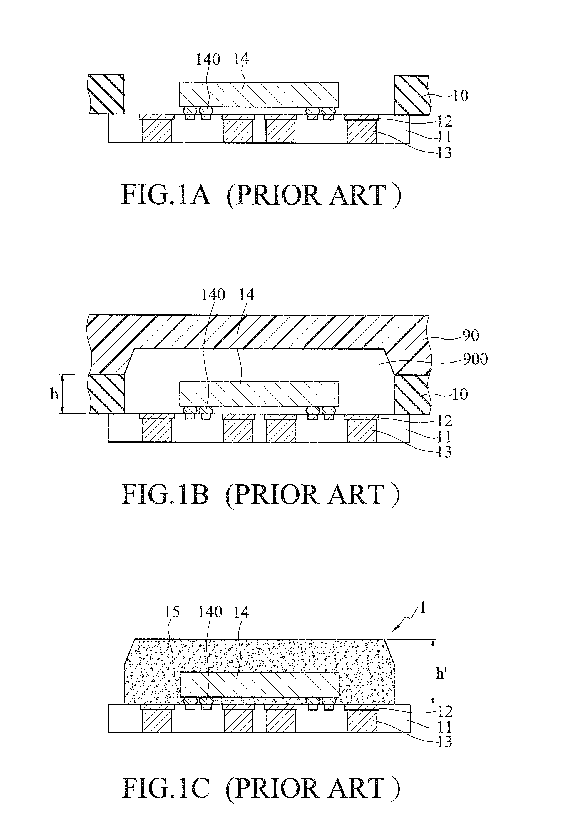
a technology of packaging and encapsulation, which is applied in the manufacture of printed circuits, cable/conductor manufacturing, metallic pattern materials, etc., can solve the problems of low production yield (units per hour, uph), difficult for the conventional package structure b>1/b> to meet the low-profile requirement, and reduce the structural height of the package. , the effect of reducing the cavity of the mold

Inactive Publication Date: 2016-03-31
SILICONWARE PRECISION IND CO LTD
View PDF4 Cites 13 Cited by
  • Summary
  • Abstract
  • Description
  • Claims
  • Application Information

AI Technical Summary

Benefits of technology

[0022]In summary, the package structure and the method of fabricating the package structure according to the present invention are characterized by forming wiring layers, conductive layers and dielectric bodies independently on two opposing surfaces of the carrier, as compared to the prior art, which forms these components on only one side of the carrier. Hence, the production yield of the package structure thus fabricated is increased by two fold, as compared to the prior art.
[0023]Moreover, the carrier is removed to prevent the need of forming a conventional supporting board, such that the cavity of the mold can be reduced according to practical needs when forming the encapsulant, thereby greatly reducing the structural height of the package and satisfying the low-profile requirement for electronic products.
[0024]In a method according to the present invention, the wiring layers and the conductive layers are formed first, the dielectric bodies are then formed, and then the conductive layers are exposed to be electrically connected to circuits that are to be formed in subsequent processes. Therefore, a laser drilling process that is used to fabricate the conductive layers on the dielectric bodies is not required, and the fabrication cost is reduced.

Problems solved by technology

However, in the method of fabricating the conventional package structure 1 since the carrier also serves as a supporting board 10, the package structure 1 can only be formed on one side of the carrier, leading to a low production yield (units per hour, UPH).
Hence, it is not possible to have a thinner encapsulant 15, and it is difficult for the conventional package structure 1 to satisfy the low-profile requirement.

Method used


Image

  • Package stucture and method of fabricating the same
  • Package stucture and method of fabricating the same
  • Package stucture and method of fabricating the same

Examples


first embodiment

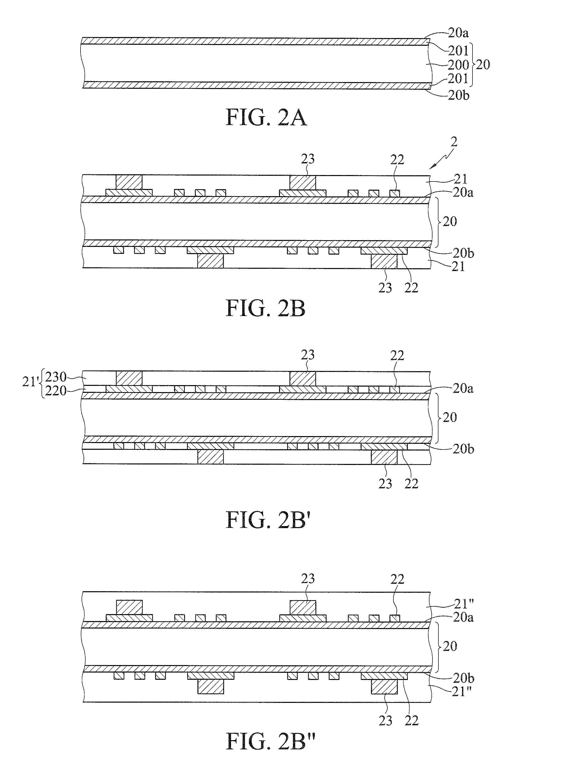
[0031]FIGS. 2A-2E are schematic cross-sectional views showing a method of fabricating a package structure 2 of a first embodiment according to the present invention.

[0032]As shown in FIG. 2A, a carrier 20 having two opposing surfaces 20a and 20b is provided.

[0033]In an embodiment, the two surfaces 20a and 20b of the carrier 20 are metal surfaces. In another embodiment, the carrier 20 has a board 200 such as a metal board, a semiconductor wafer or a glass board, and a metal layer 201 is formed on two opposing sides of the board 200. The metal layer 201 is a copper foil. In yet another embodiment, a release film, an adhesive or an insulating material can be disposed between the board 200 and the metal layer 201 according to practical requirements, so as to facilitate the latter separation process.

[0034]As shown in FIG. 2B, two dielectric bodies 21 are formed on the two surfaces 20a and 20b of the carrier 20, respectively, and each of the dielectric bodies 21 has a first wiring layer 2...

second embodiment

[0052]FIGS. 3A-3D are schematic cross-sectional views showing a method of fabricating a package structure 3 of a second embodiment according to the present invention.

[0053]As shown in FIG. 3A, a structure similar to the structure shown in FIG. 2B is provided.

[0054]In the second embodiment, the structure of FIG. 3A can be fabricated according to the processes shown in FIGS. 2A and 2B.

[0055]As shown in FIG. 3B, second wiring layers 32 are formed on the dielectric bodies 21 by a patterning process, and are electrically connected to the first conductive layers 23.

[0056]As shown in FIG. 3C, insulation protection layers 31 on the dielectric bodies 21 and the second wiring layers 32.

[0057]In an embodiment, the second wiring layers 32 are exposed from surfaces of the insulation protection layers 31. In fabrication, the insulation protection layers 31 are pressed on the dielectric bodies 21, with the second wiring layers 32 free from being exposed from the surfaces of the insulation protecti...

third embodiment

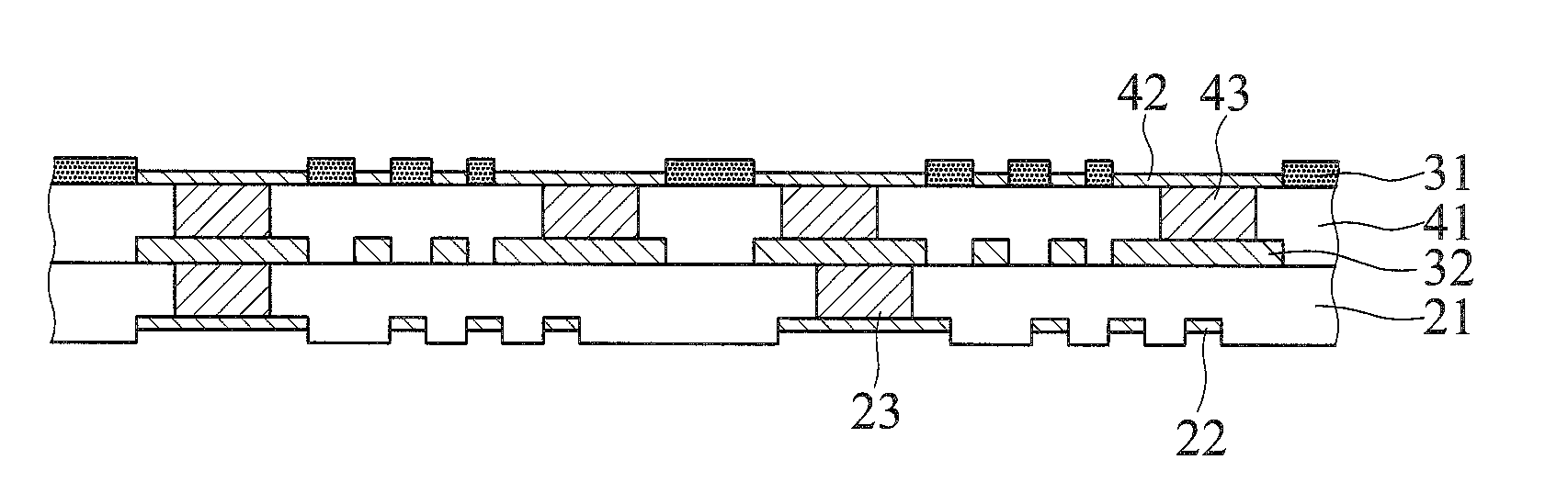
[0061]FIGS. 4A-4E are schematic cross-sectional views showing a method of fabricating a package structure 4 of a third embodiment according to the present invention.

[0062]As shown in FIG. 4A, the process thereof subsequent to the process shown in FIG. 2B, second wiring layers 32 are formed on the dielectric bodies 21 and electrically connected to the first conductive layers 23, and second conductive layers 43 are formed on a portion of surfaces of the second wiring layers 32.

[0063]In an embodiment, the second wiring layers 32 are formed on the dielectric bodies via a first resist layer, the second conductive layers 43 are then formed on the portion of the surfaces of the second wiring layers 32 via a second resist layer, and finally the first and second resist layers are removed.

[0064]As shown in FIG. 4B, dielectric layers 41 are formed on the dielectric bodies 21, and encapsulate the second wiring layers 32 and the second conductive layers 43.

[0065]In an embodiment, the dielectric ...


PUM


Abstract

A method of fabricating a package structure is provided. The method includes providing a carrier having two opposing surfaces, forming dielectric bodies on the two surfaces of the carrier, respectively, each of the dielectric bodies having a wiring layer embedded therein and a conductive layer formed on the wiring layer, and removing the carrier. Therefore, the wiring layers, the conductive layers and the dielectric bodies are formed on the two surfaces of the carrier, respectively, and the production yield is thus increased. The present invention further provides the package structure thus fabricated.

Description

BACKGROUND OF THE INVENTION[0001]1. Field of the Invention[0002]The present invention relates to package structures, and, more particularly, to a circuit package structure of a semiconductor package and a method of fabricating the same.[0003]2. Description of Related Art[0004]With the rapid growth in electronic industry, high-end electronic products have been developed to have a compact size and a low profile. As the packaging technology advances, an increasing number of different types of chip packaging technologies have been developed, as well as the size of the semiconductor package is continuously decreasing in order to achieve the low-profile requirement for the semiconductor package.[0005]FIGS. 1A-1C are cross-sectional views showing a method of fabricating a conventional package structure 1.[0006]As shown in FIG. 1A, a dielectric body 11 is formed on a carrier, and a wiring layer 12 and a conductive layer 13 formed on the wiring layer 12 are embedded in the dielectric body 11...

Claims


Application Information

Patent Timeline
Patent Type & Authority Applications(United States)
IPC IPC(8): H01L23/13H01L21/48H01L21/56H01L23/00
CPCH01L23/13H01L24/83H01L21/563H01L21/481H01L2924/37001H01L23/3128H01L24/13H01L24/16H01L24/32H01L24/48H01L24/73H01L24/92H01L2224/131H01L2224/13147H01L2224/16235H01L2224/16237H01L2224/32225H01L2224/48227H01L2224/73204H01L2224/92125H01L2924/15311H01L2924/1579H05K3/4682H05K2203/0152H05K2203/016H01L2924/00014H01L23/498H01L23/49822H01L21/4857H01L2924/014H01L2224/45099H01L2224/45015H01L2924/207H01L2224/16225H01L2924/00
Inventor PAI, YU-CHENGCHIU, SHIH-CHAOLIN, CHUN-HSIENFAN, CHIH-WENCHEN, CHENG-CHIA
Owner SILICONWARE PRECISION IND CO LTD
Why Eureka
Try Eureka