Methods for forming vertical semiconductor pillars

a technology of vertical semiconductor pillars and manufacturing methods, applied in the field of semiconductor device structure and manufacturing methods, to achieve the effect of reducing the roughness of the line edg

Active Publication Date: 2016-03-31
SEMICONDUCTOR MANUFACTURING INTERNATIONAL (BEIJING) CORP +1
View PDF5 Cites 3 Cited by
  • Summary
  • Abstract
  • Description
  • Claims
  • Application Information

AI Technical Summary

Benefits of technology

[0004]The inventors have identified drawbacks in the conventional methods for forming vertical nanowire structures, such as bending profiles. Embodiments of the present invention provide a method for forming vertical nanowires without the bending profiles while allowing reduced line edge roughness through annealing. Further, the annealing process can be performed at a higher temperature and / or for a longer period of time to allow more rounded profiles to form circular or elliptical nanowires.

Problems solved by technology

The inventors have identified drawbacks in the conventional methods for forming vertical nanowire structures, such as bending profiles.

Method used


Image

  • Methods for forming vertical semiconductor pillars
  • Methods for forming vertical semiconductor pillars
  • Methods for forming vertical semiconductor pillars

Examples


Embodiment Construction

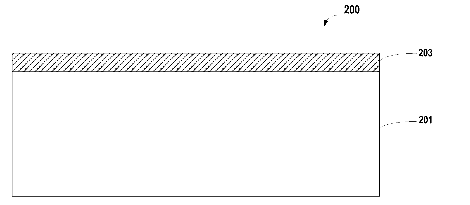
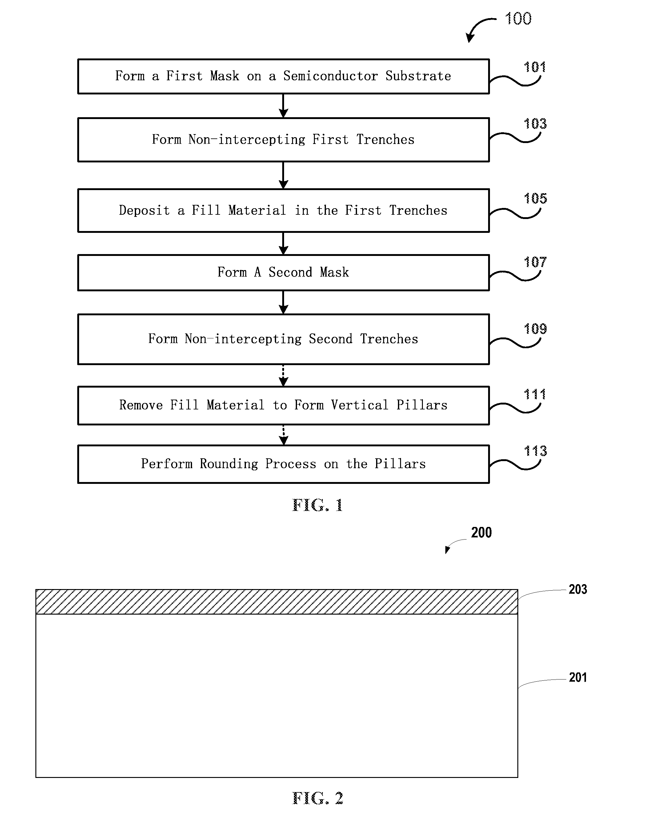
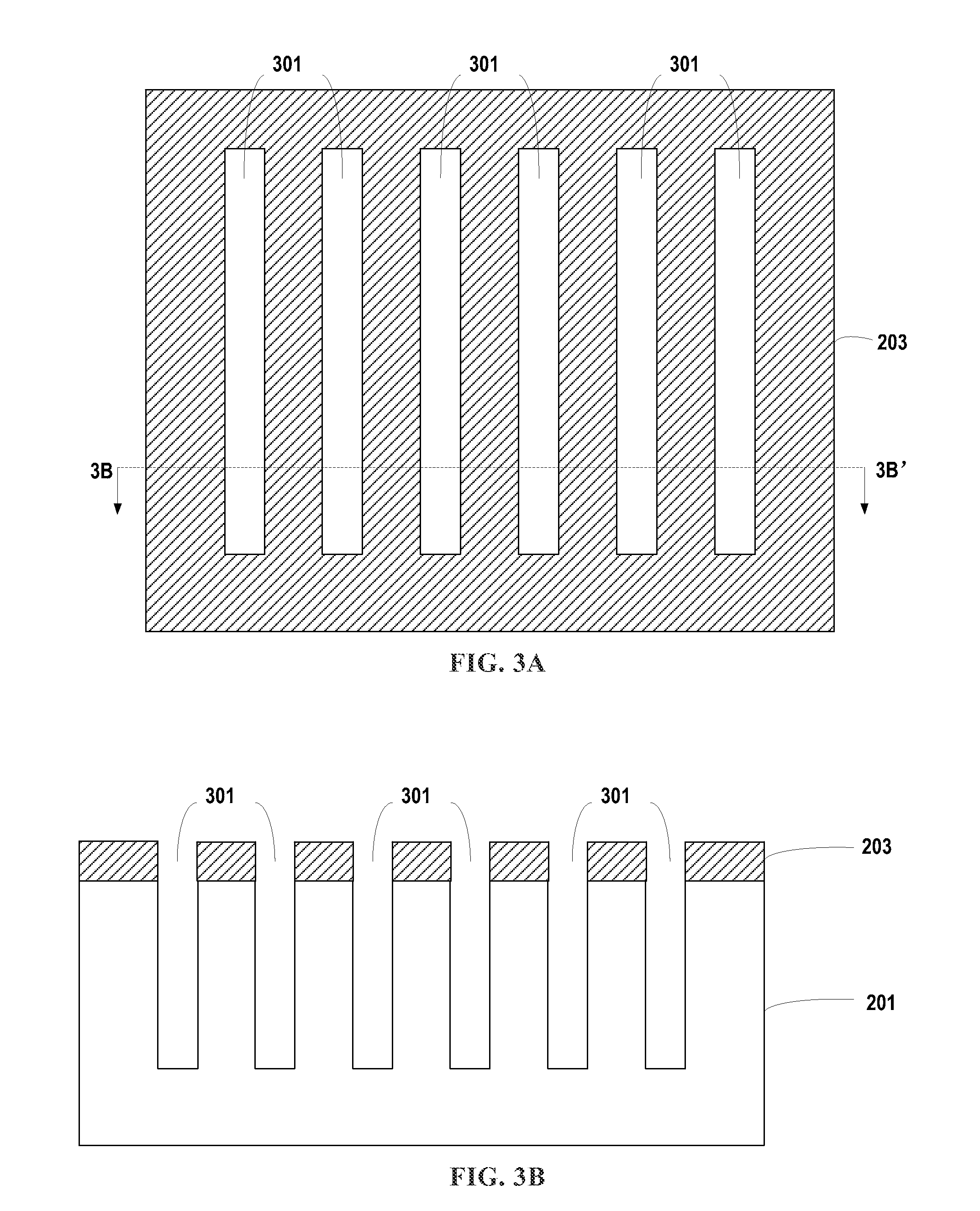
[0012]Exemplary embodiments of the present invention will be described with reference to the figures. The following description of exemplary embodiments is illustrative only, and not intended to be any limitation on the invention and its application or use. It is understood that the relative arrangement of parts and steps and numeric expressions set forth in these embodiments are not to be construed as limiting the scope of the invention. It is also understood that, for convenience of description, the size of the various components shown in the drawings are not necessarily drawn in actual proportional relationship. Techniques, methods and devices known to one of ordinary skill in the relevant art may not be discussed in detail, but in situations in which these techniques, methods and apparatus apply, these techniques, methods and apparatus should be considered as part of this specification. Further, similar reference numerals and letters are used to refer to similar items in the fol...


PUM


Abstract

A method for forming a semiconductor device includes providing a semiconductor structure, which includes a semiconductor substrate and a first mask layer on the substrate. The first mask layer is used to form a plurality of first trenches that extends into the substrate and extends laterally in a first direction and do not intersect each other. The first trenches are then filled with a fill material. Next, a second mask layer is formed on the semiconductor structure filled with the fill material. The second mask layer is then used to form a second plurality of trenches in the semiconductor substrate that extend laterally in a second direction and do not intersect each other. Each of the second trenches intersects at least one of the first plurality of trenches. Next, the fill material is removed to form a plurality of vertical pillars defined by intersecting first trenches and second trenches.

Description

CROSS-REFERENCES TO RELATED APPLICATIONS[0001]This application claims priority to Chinese patent application No. 201410500240.8, filed on Sep. 26, 2014, the content of which is incorporated herein by reference in its entirety.BACKGROUND OF THE INVENTION[0002]The present invention relates to the field of semiconductor technology. Specifically, embodiments of the invention are directed to semiconductor device structures and manufacturing methods.[0003]Vertical nanowire devices have been used for three-dimensional (3D) memory devices and they can also be used in logic devices. The inventor has observed that, in conventional vertical nanowire devices, the annealing process tends to result in a bending profile.BRIEF SUMMARY OF THE INVENTION[0004]The inventors have identified drawbacks in the conventional methods for forming vertical nanowire structures, such as bending profiles. Embodiments of the present invention provide a method for forming vertical nanowires without the bending profi...

Claims


Application Information

Patent Timeline
Patent Type & Authority Applications(United States)
IPC IPC(8): H01L29/06H01L21/306H01L21/3065H01L21/308
CPCH01L29/0676H01L21/3065H01L21/30625H01L21/3086H01L21/3081B82Y30/00H01L21/3083
Inventor HONG, ZHONGSHAN
Owner SEMICONDUCTOR MANUFACTURING INTERNATIONAL (BEIJING) CORP
Why Eureka
Try Eureka