

Photosensitive polymer, photoresist composition including the photosensitive polymer and method of forming a photoresist pattern using the photoresist composition
Inactive Publication Date: 2006-06-22
SAMSUNG ELECTRONICS CO LTD
View PDF4 Cites 3 Cited by
- Summary
- Abstract
- Description
- Claims
- Application Information
AI Technical Summary
Benefits of technology
[0013] Certain embodiments of the present invention provide a photosensitive polymer having good reproducibility and high resolution.
[0019] According to the present invention, a photoresist composition may prevent a development difference of a photoresist film due to a different wetting time of each portion of the photoresist film with a developing solution. Thus, a photoresist pattern having a uniform thickness may be obtained. Furthermore, when a photoresist pattern is formed using the photoresist composition of the present invention, the photoresist pattern may reduce line edge roughness and an extremely fine pattern may be formed with accuracy. Therefore, a defect generation of a semiconductor device may be prevented and a productivity of a semiconductor manufacturing process may be enhanced.
Problems solved by technology
As semiconductor manufacturing processes become more complicated and the degree of integration of a semiconductor device increases, a photoresist composition used for forming an extremely fine pattern is required.
However, the dry-etching resistance of the photoresist is not sufficiently enhanced, and a line-edge roughness (LER) of the photoresist pattern that is formed using the copolymer is observed.
However, the alternate copolymer is prepared in very low yield.
Method used
View moreImage
Smart ImageViewing Examples

Examples
example
[0066] A photoresist composition was prepared by mixing about 4 percent by weight of a photosensitive polymer of the present invention, about 0.3 percent by weight of sulfonate as a photosensitive material, about 0.15 percent by weight of trimethylamine as an organic base, about 0.55 percent by weight of ethylene glycol as an additive, and about 95 percent by weight of an organic solvent including propylene glycol methyl ether and ethyl lactate in a weight ratio of about 8:2.
Login to View More PUM
 Abstract
In a photosensitive polymer, a photoresist composition including the photosensitive polymer and a method of forming a photoresist pattern using the photoresist composition, the photosensitive polymer has a weight average molecular weight of from about 1,000 up to about 100,000 and a repeating unit represented by the following chemical formula (1). wherein R1 represents hydrogen or an alkyl group having 1 to 10 carbon atoms, R2 represents an acid-labile hydrocarbon group having 3 to 12 carbon atoms, and n represents an integer greater than or equal to 1. The photoresist composition having good reproducibility and stability may form a photoresist film having a substantially uniform thickness, and may form a fine pattern with accuracy.
Description
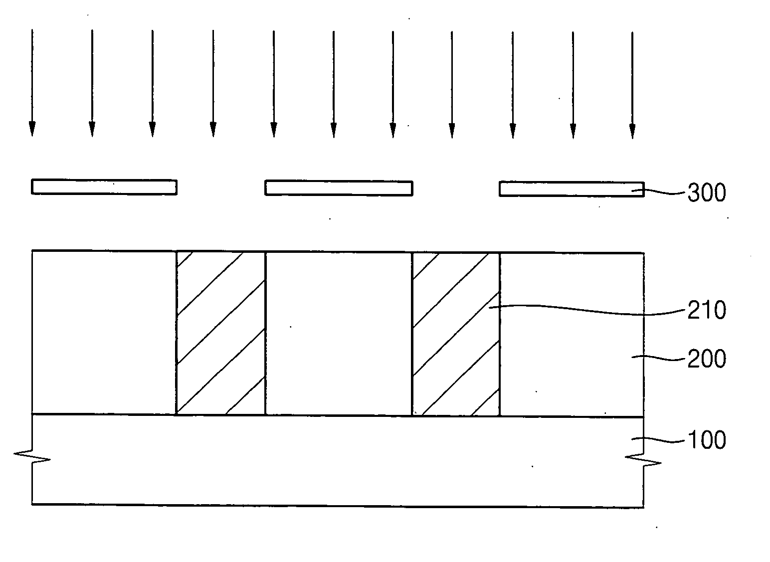
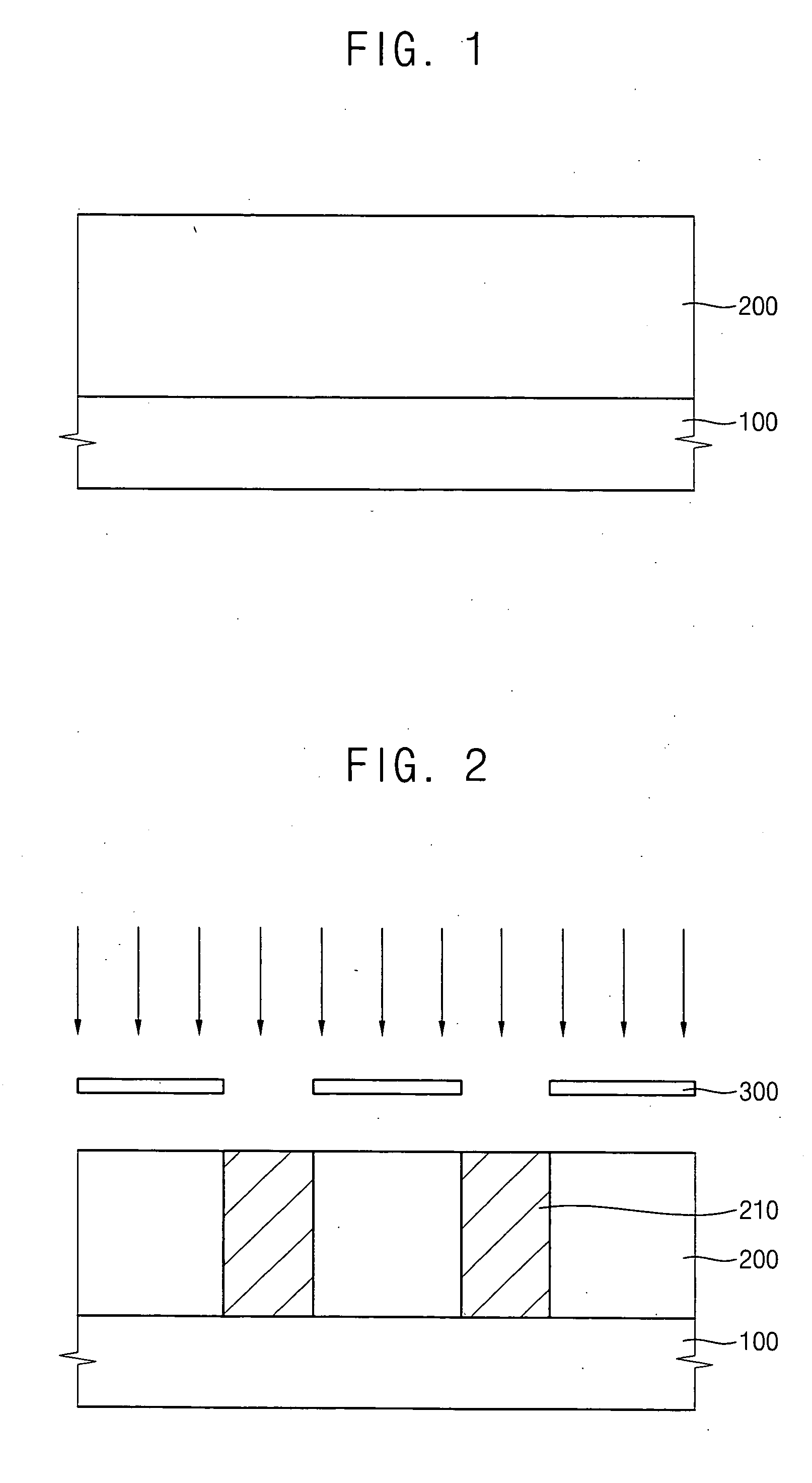
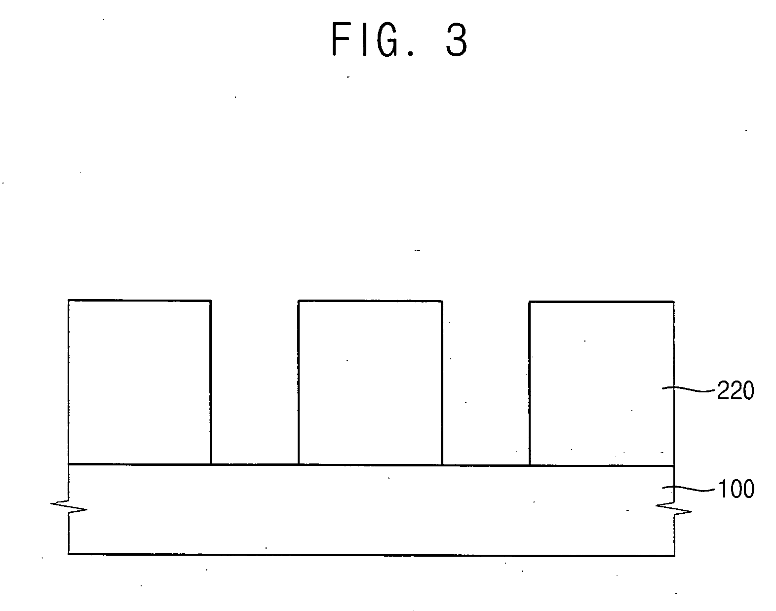
CROSS REFERENCE TO RELATED APPLICATIONS [0001] This application claims priority under 35 USC § 119 to Korean Patent Application No. 2004-107663 filed on Dec. 17, 2004, the contents of which are herein incorporated by reference in its entirety. BACKGROUND OF THE INVENTION [0002] 1. Field of the Invention [0003] The present invention relates to a photosensitive polymer. More particularly, the present invention relates to a photosensitive polymer for forming a pattern in a semiconductor manufacturing process, a photoresist composition including the photosensitive polymer and a method of forming a photoresist pattern using the photoresist composition. [0004] 2. Description of the Related Art [0005] Semiconductor devices having a high degree of integration and a rapid response speed are increasingly desirable as information processing apparatuses have been developed. Hence, the technology of manufacturing these semiconductor devices has been developed to improve the degree of integration...
Claims
Login to View More Application Information
Patent Timeline
 IPC IPC(8): G03C1/76
CPCG03F7/0392G03F7/039
InventorMOON, SANG-SIK
OwnerSAMSUNG ELECTRONICS CO LTD