Method for forming an electronic device

a technology of electronic devices and etching, applied in the direction of semiconductor devices, basic electric elements, electrical equipment, etc., can solve the problems of polysilicon etching, gate line roughness, gate length variation, etc., to reduce the variation in gate length, and reduce the line edge roughness

Inactive Publication Date: 2005-04-26
GLOBALFOUNDRIES INC
View PDF47 Cites 9 Cited by
  • Summary
  • Abstract
  • Description
  • Claims
  • Application Information

AI Technical Summary

Benefits of technology

[0007]In general, the present invention provides a method for forming an electronic device such as a FET device. Specifically, under the present invention, a layer of amorphous silicon is formed over a layer of gate dielectric. After the layer of amorphous silicon is formed, a gate cap dielectric is deposited. Implantation of dopants is then performed as needed. Thereafter, gate lines are patterned lithographically and the gate cap dielectric, amorphous silicon, and gate dielectric are etched to form the gate lines. It should be noted that the state of silicon is amorphous at the time of etching to minimize the line edge roughness. The absence of grain boundaries, which would be present in polysilicon, reduces the line edge roughness at the time of etching. Further, the amorphous silicon is confined on the top by gate cap dielectric and on the bottom by gate dielectric. The sides of amorphous silicon are then confined by at least one spacer, which is deposited under a low temperature process. Low temperature processing in this manner preserves the chrystallographical state of the amorphous silicon material throughout the spacer deposition(s). Once the at least one spacer is in place, the amorphous silicon is exposed to a temperature sufficiently high to convert the amorphous silicon to polysilicon. By waiting until the amorphous silicon is confined within the at least one spacer before converting it to polysilicon, the movement of the silicon atoms within the silicon material is confined within the at least one spacer laterally and the variation in gate length is reduced.

Problems solved by technology

However, a prevailing cause of gate length variation is the grain structure of polycrystalline silicon.
The grain-like structure of the polysilicon typically causes gate line roughness during polysilicon etching.
Exposure of the amorphous silicon to high temperatures causes structural transformation, which when occurring in an unconfined environment, cause movement of the silicon material during the polysilicon grain growth.
Thus, the roughness of the gate silicon line is increased, which leads to variation in the gate length.
Such a variation in gate length 14 can raise significant performance issues in the device.

Method used


Image

  • Method for forming an electronic device
  • Method for forming an electronic device
  • Method for forming an electronic device

Examples


Embodiment Construction

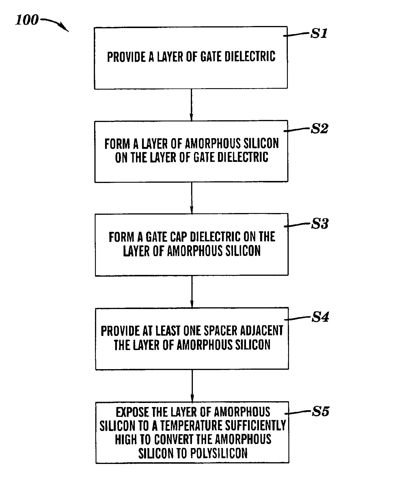
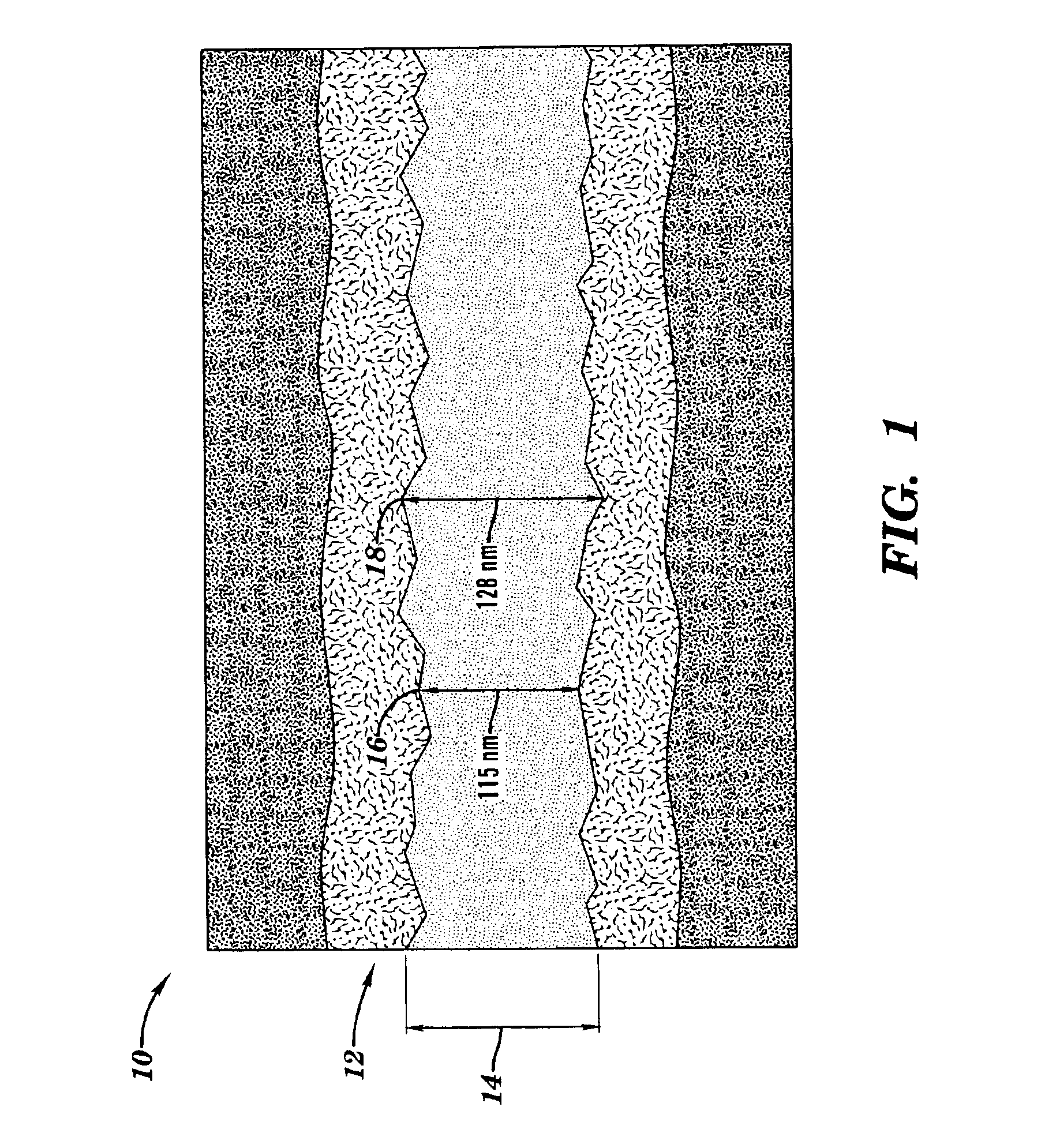
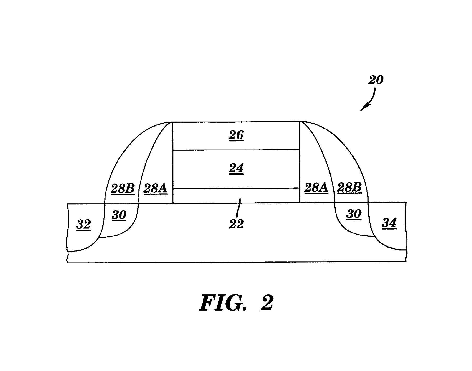
[0018]As indicated above, the present invention provides a method for forming an electronic device such as a FET device. Specifically, under the present invention, a layer of amorphous silicon is formed over a layer of gate dielectric. After the layer of amorphous silicon is formed, a gate cap dielectric is deposited. Implantation of dopants is then performed as needed. Thereafter, gate lines are patterned lithographically and the gate cap dielectric, amorphous silicon, and gate dielectric are etched to form the gate lines. It should be noted that the state of silicon is amorphous at the time of etching to minimize the line edge roughness. The absence of grain boundaries, which would be present in polysilicon, reduces the line edge roughness at the time of etching. Further, the amorphous silicon is confined on the top by gate cap dielectric and on the bottom by gate dielectric. The sides of amorphous silicon are then confined by at least one spacer, which is deposited under a low te...


PUM

PropertyMeasurementUnit
temperatureaaaaaaaaaa
gate lengthaaaaaaaaaa

Abstract

Under the present invention, a layer of amorphous silicon is formed over a layer of gate dielectric. Over the layer of amorphous silicon, a gate cap dielectric is formed. The layer of amorphous silicon is then confined by at least one spacer, which is deposited under a low temperature process. Once the at least one spacer is in place, the amorphous silicon is exposed to a temperature sufficiently high to convert the amorphous silicon to polysilicon. By waiting until the amorphous silicon is confined within the at least one spacer before converting it to polysilicon, the variation in gate length is reduced.

Description

BACKGROUND OF THE INVENTION[0001]1. Field of the Invention[0002]The present invention generally relates to a method for forming an electronic device such as a field-effect transistor (FET) device. Specifically, the present invention relates to a method for forming an electronic device in which gate length variation is reduced.[0003]2. Related Art[0004]In the process of manufacturing electronic devices such as FET devices, several factors can lead to gate length variation. One such factor is the incapability of the lithographic tools to produce straight edge gate lines. Another factor is the etching process whereby uneven gate lines are produced. However, a prevailing cause of gate length variation is the grain structure of polycrystalline silicon. Specifically, in the manufacture of many electronic devices such as FET devices, the gate polysilicon is deposited as polycrystalline silicon. The grain-like structure of the polysilicon typically causes gate line roughness during polysili...

Claims


Application Information

Patent Timeline
Patent Type & Authority Patents(United States)
IPC IPC(8): H01L21/02H01L21/70H01L21/336H01L21/8238H01L21/28H01L29/49
CPCH01L21/28035H01L29/6656H01L29/4925
Inventor BALASUBRAMANYAM, KARANAMBIESEMANS, SERGEPARK, BYEONGJU
Owner GLOBALFOUNDRIES INC
Why Eureka
Try Eureka