Method for forming semiconductor structure with reduced line edge roughness

a technology of semiconductor structure and line edge roughness, which is applied in the field of semiconductor structure forming with reduced line edge roughness, can solve the problems of inaccurate metrology and adversely affect device performance, and achieve the effect of reducing line edge roughness (ler)

Inactive Publication Date: 2013-03-28
NAN YA TECH
View PDF3 Cites 2 Cited by
  • Summary
  • Abstract
  • Description
  • Claims
  • Application Information

AI Technical Summary

Benefits of technology

[0010]Therefore, a method for forming a semiconductor structure with reduced line edge roughness (LER) is provided.

Problems solved by technology

Moreover, as feature size decreases, line-edge roughness can interfere with accurate metrology and adversely affect device performance.

Method used


Image

  • Method for forming semiconductor structure with reduced line edge roughness
  • Method for forming semiconductor structure with reduced line edge roughness
  • Method for forming semiconductor structure with reduced line edge roughness

Examples


example 1

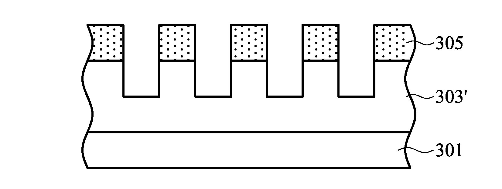
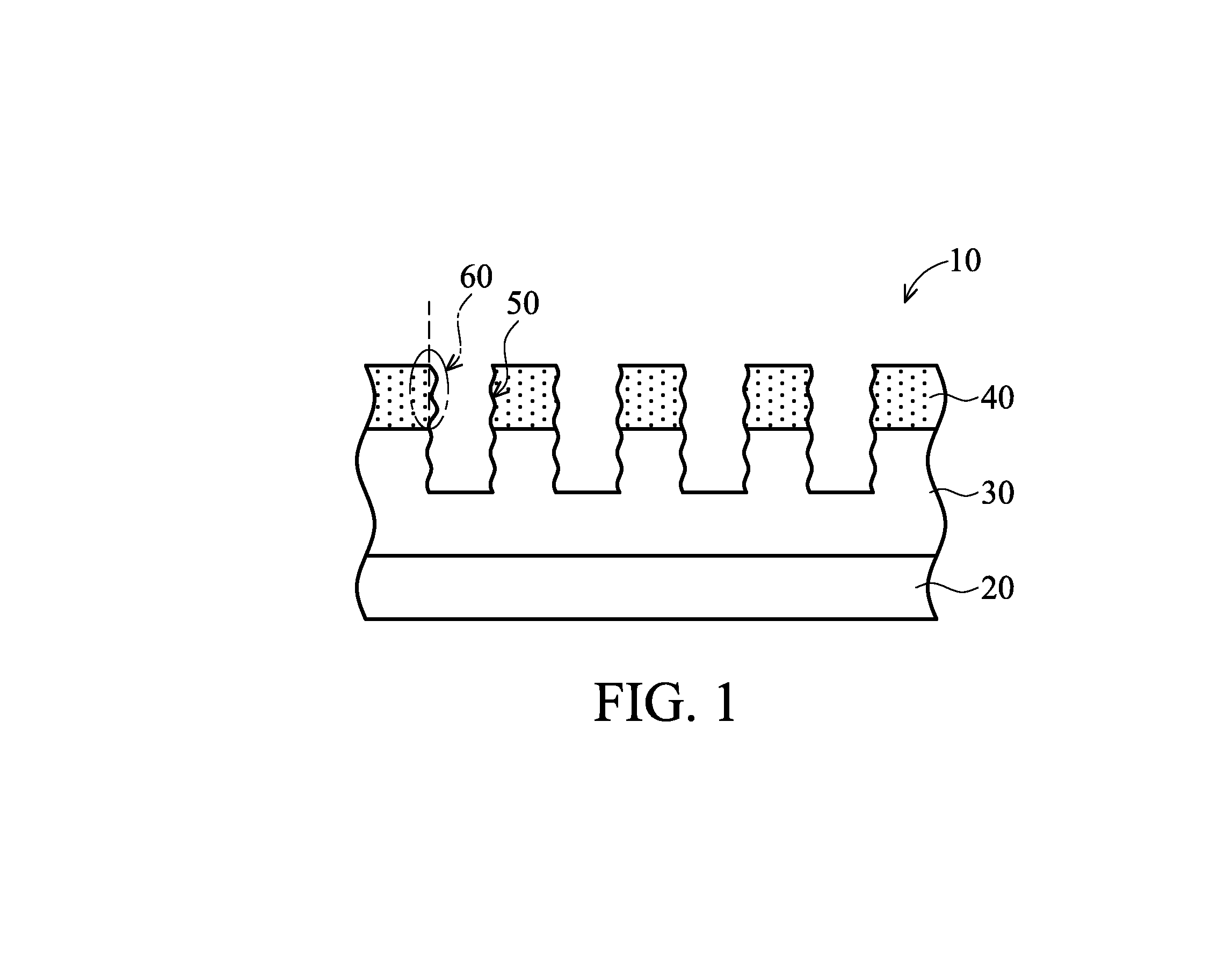
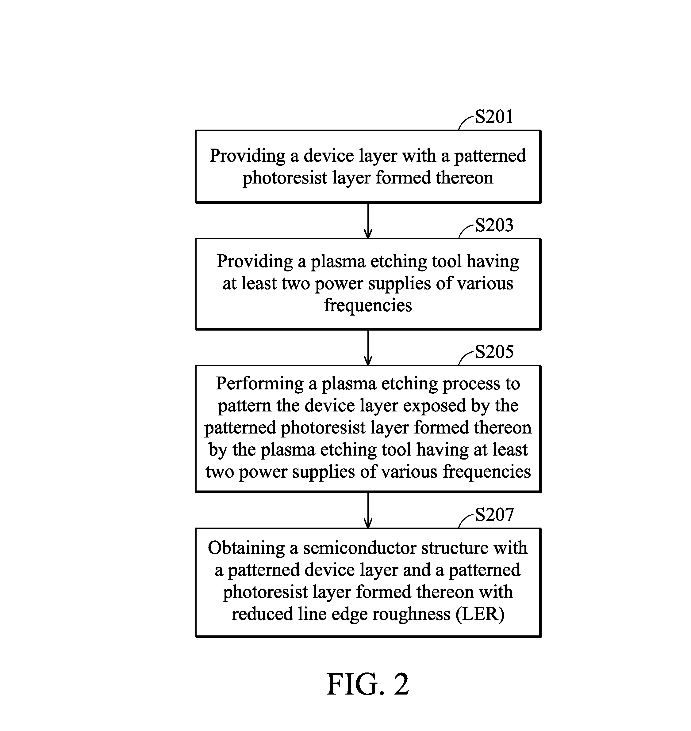
[0025]A semiconductor device similar with that shown in FIG. 3 was provided. The semiconductor device was formed with a silicon oxide layer and a patterned photoresist layer formed thereover. The patterned photoresist layer was formed with a width of about 40 nm. Next, a plasma etching was performed to etch the silicon oxide layer by an inductively coupled plasma (ICP) etching tool, using etchants comprising CHF3, O2 and argon (Ar). The (ICP) etching tool comprises two power supplies operated in a frequency of 2 MHz and 13.56 MHz, respectively, and the power supply of the frequency of 13.56 MHz in the plasma etching tool was operated under a continuous on-stage voltage during the plasma etching and the power supply of the lower frequency of the 2 MHz frequency in the plasma etching tool was operated under an on-off stage voltage with pulsing modulation during the plasma etching process. An on-time interval of the on-off stage voltage was less than 1E-6 seconds, and the power supplie...


PUM

PropertyMeasurementUnit
frequencyaaaaaaaaaa
frequencyaaaaaaaaaa
timeaaaaaaaaaa

Abstract

A method for forming a semiconductor structure with reduced line edge roughness is provided, including: providing a device layer with a patterned photoresist layer formed thereon; and performing a plasma etching process to pattern the device layer with the patterned photoresist layer formed thereon, forming a patterned device layer, wherein the plasma etching process is operated under a continuous on-stage voltage provided with a relative higher frequency and an on-off stage voltage with pulsing modulation provided with a relative lower frequency.

Description

BACKGROUND OF THE INVENTION[0001]1. Field of the Invention[0002]The invention relates to semiconductor fabrication, and in particularly to a method for forming a semiconductor structure with reduced line edge roughness (LER).[0003]2. Description of the Related Art[0004]Generally, photolithography techniques are applied in the process of manufacturing semiconductor devices. Photolithography techniques are composed of the following steps. First, a photoresist material is applied on laminated thin film layers disposed on a semiconductor substrate, which is exposed to ultra violet rays in an exposure apparatus. Thereby, the circuit pattern of a photoresist mask is transferred onto the photoresist material via exposure, which is then developed. Thereafter, the desired circuit pattern is formed via an etching process using plasma.[0005]Furthermore, a plasma processing apparatus is generally used for the etching process for transferring the developed photoresist circuit pattern to the lami...

Claims


Application Information

Patent Timeline
Patent Type & Authority Applications(United States)
IPC IPC(8): H01L21/3065
CPCB23K26/00H01L21/31116B23K10/003B23K2101/40
Inventor WU, CHANG-MINGCHEN, YI-NANLIU, HSIEN-WEN
Owner NAN YA TECH
Why Eureka
Try Eureka