

Light source, method for manufacturing the light source, and method for mounting the light source
a technology for light sources and light sources, which is applied in the direction of semiconductor/solid-state device manufacturing, electrical equipment, semiconductor devices, etc., can solve the problem that solder balls made of solder balls cannot provide sufficient bonding strength, and achieve the effect of high bonding strength
- Summary
- Abstract
- Description
- Claims
- Application Information
AI Technical Summary
Benefits of technology
Problems solved by technology
Method used
Image

Examples
first representative embodiment
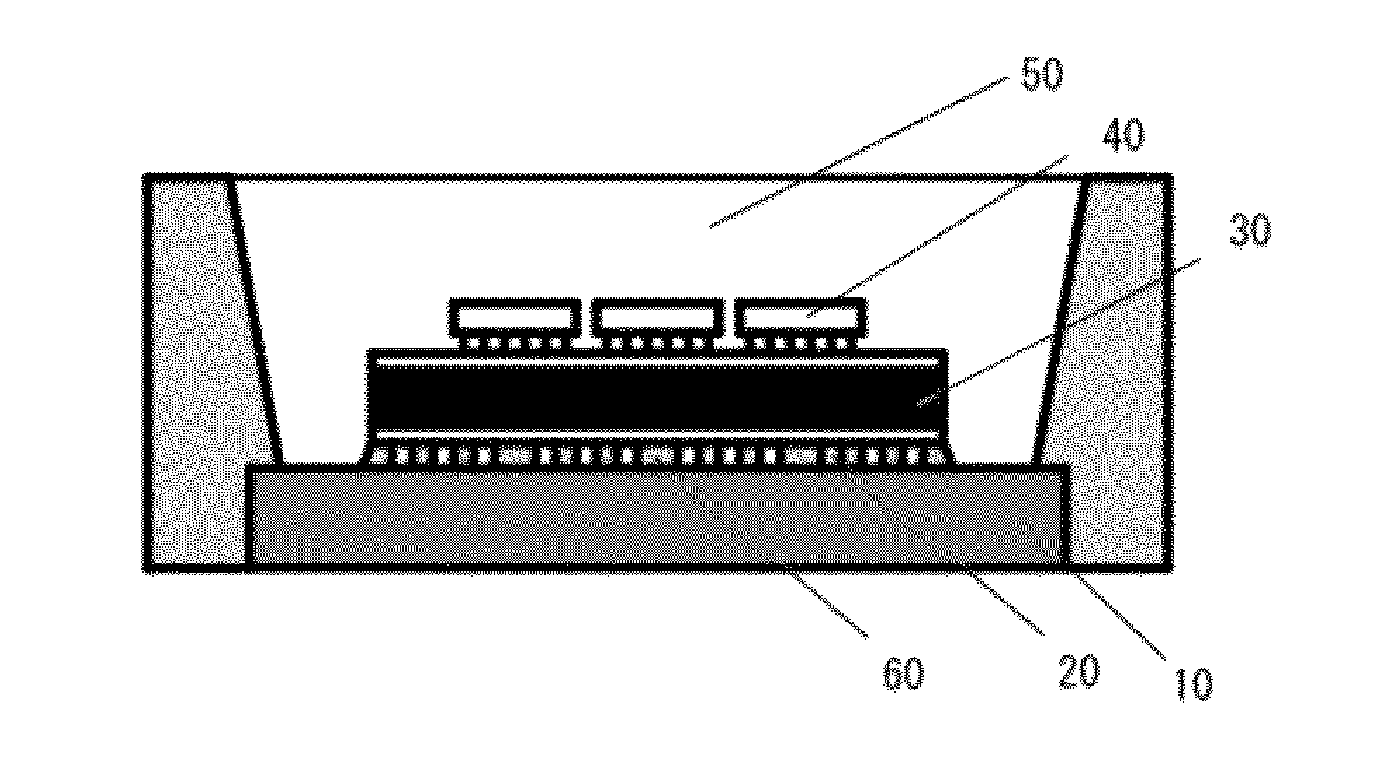
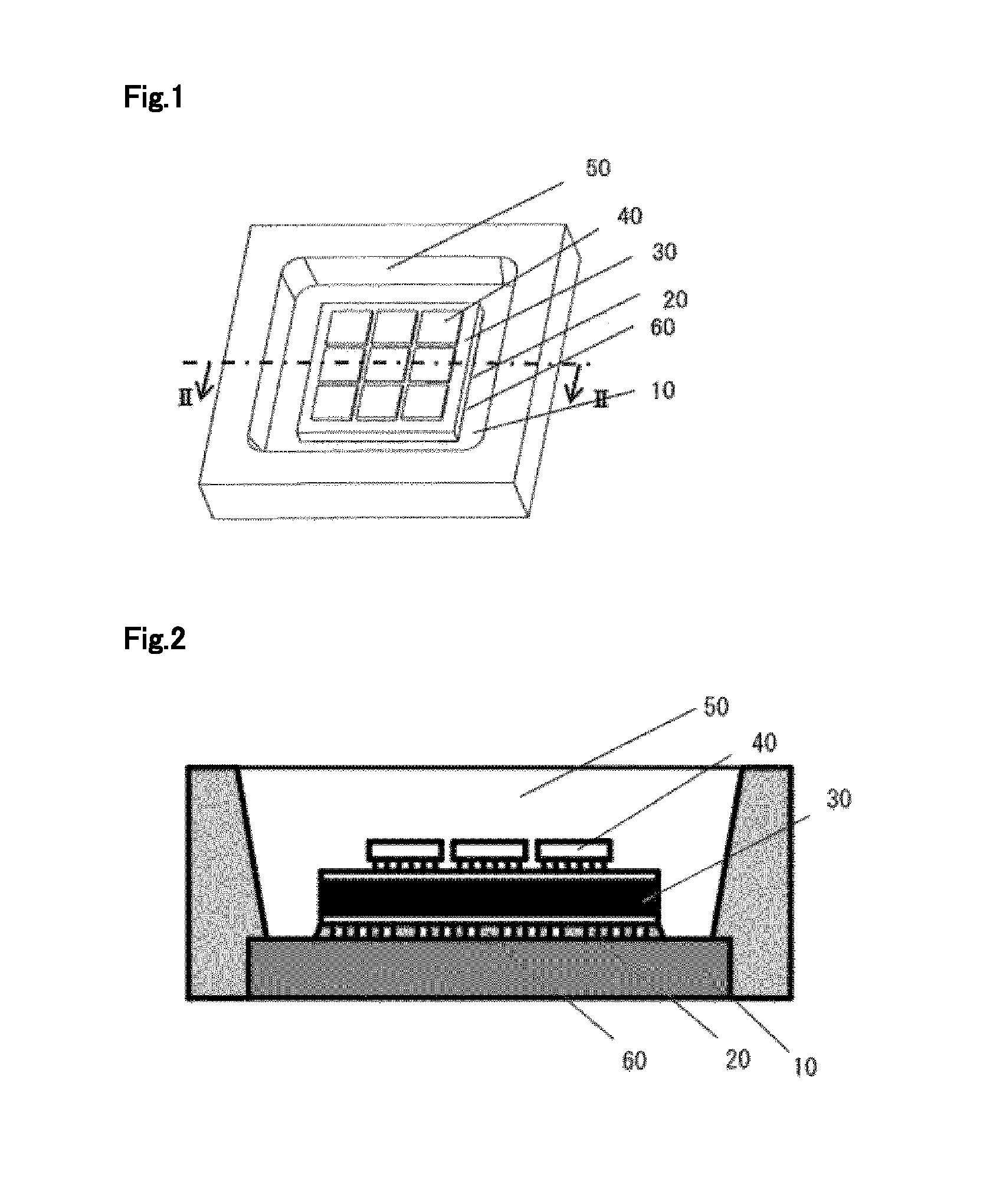
[0029]A light source according to a first embodiment will be described below with reference to the drawings. FIG. 1 is a schematic perspective view showing the light source according to the first embodiment. FIG. 2 is a schematic cross-sectional view, taken along line II-II in FIG. 1, showing the light source according to the first embodiment.
[0030]The light source includes a mounting substrate 10, metal bumps 20, a ceramic substrate 30, light-emitting elements 40, and a sealing member 50.
[0031]The mounting substrate 10 is an approximately rectangular parallelepiped member formed in a cup-shape having a bottom surface and side surfaces, and defining an opening. In a plan view, a periphery defining the opening of the cup-shaped portion has a quadrangular shape with rounded corners. The mounting substrate 10 can be formed with a copper material and a thermoplastic resin. For the thermoplastic resin, a polyphthalamide, a liquid crystal polymer, a polybutylene terephthalate (PBT), an un...
second representative embodiment
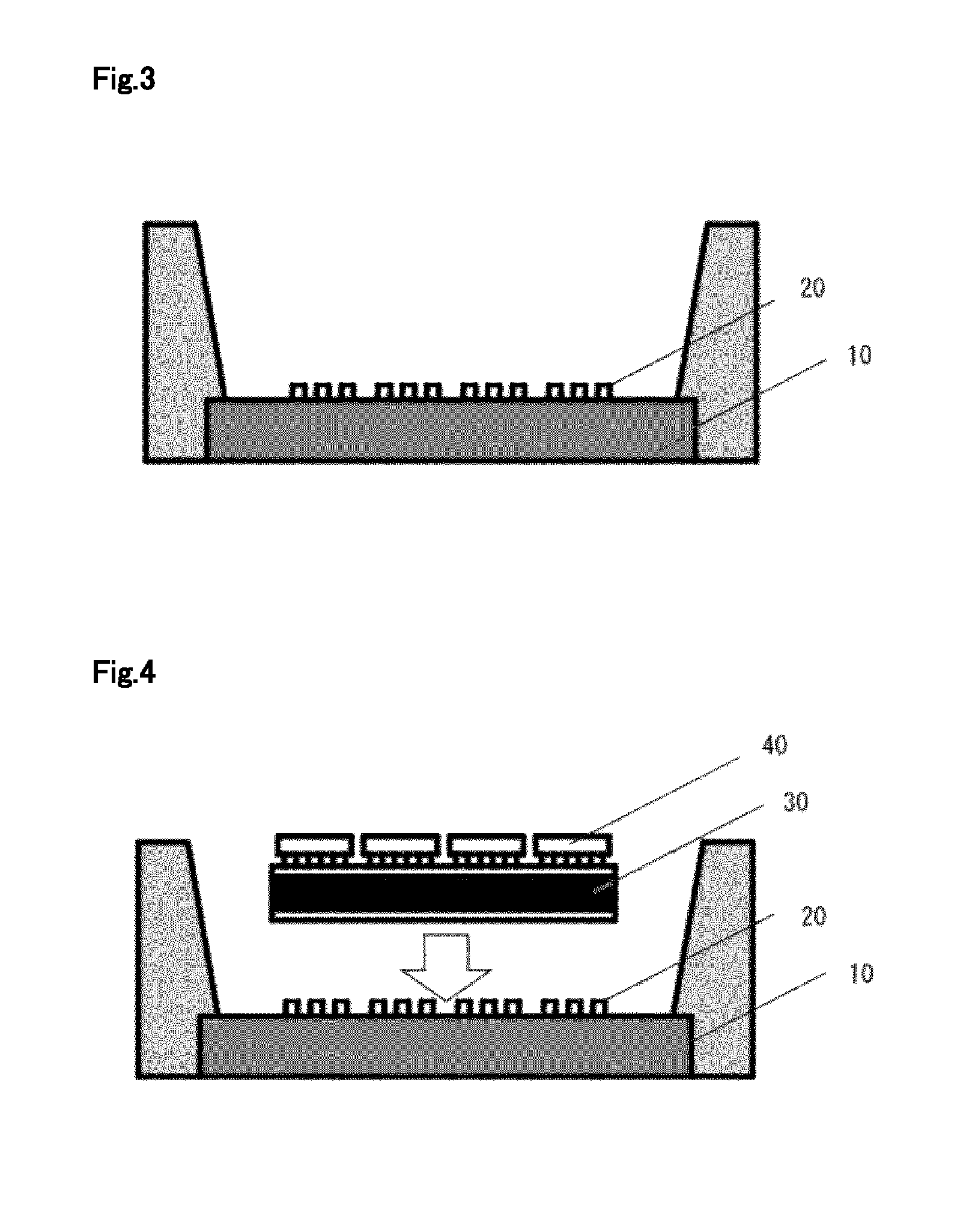
[0049]In place of the method of manufacturing a light source according to the first embodiment, the light source according to the first embodiment can be manufactured by a method of manufacturing a light source according to a second embodiment. FIG. 7 is a schematic cross-sectional view showing the process of manufacturing a light source according to the second embodiment.
[0050]First, a plurality of metal bumps 20 are formed on the mounting substrate 10.
[0051]Next, the ceramic substrate 30 is placed on the mounting substrate 10, and the mounting substrate 10 and the ceramic substrate 30 are bonded to each other via the metal bumps 20.
[0052]Next, the light-emitting elements 40 are mounted on the ceramic substrate 30.
[0053]Next, the resin 60 is poured into the gap between the mounting substrate 10 and the ceramic substrate 30.
[0054]Next, the light-emitting elements 40 on the ceramic substrate 30 are covered with the sealing member 50.
[0055]The light-emitting elements 40 are mounted on...
third representative embodiment
[0056]In place of the method of manufacturing a light source according to the first embodiment, the light source according to the first embodiment can be manufactured by a method of manufacturing a light source according to a third embodiment. FIG. 8 is a schematic cross-sectional view showing the process of manufacturing a light source according to the third embodiment.
[0057]A plurality of metal bumps 20 made of gold, copper, a gold alloy or a copper alloy are formed on the ceramic substrate 30. The metal bumps 20 are formed on the back surface side of the ceramic substrate 30.
[0058]The ceramic substrate 30 is placed on the mounting substrate 10, and the mounting substrate 10 and the ceramic substrate 30 are bonded to each other via the metal bumps 20.
[0059]The light-emitting elements 40 are mounted on the ceramic substrate 30.
[0060]The metal bumps 20 are formed on the ceramic substrate 30 side, so that the alignment control between the ceramic substrate 30 and the mounting substra...
PUM
| Property | Measurement | Unit |
|---|---|---|
| height | aaaaa | aaaaa |
| diameter | aaaaa | aaaaa |
| temperature | aaaaa | aaaaa |
Abstract
Description
Claims
Application Information