Semiconductor device and method for fabricating the same

a technology of semiconductors and transistors, applied in the direction of semiconductor devices, transistors, electrical equipment, etc., can solve the problems of deterioration of performance and yield of subsequent processes performed on the surface of finfet structures, affecting the performance and yield of subsequent processes, and affecting the performance of the finfet structur

Active Publication Date: 2016-04-07
UNITED MICROELECTRONICS CORP
View PDF5 Cites 54 Cited by
  • Summary
  • Abstract
  • Description
  • Claims
  • Application Information

AI Technical Summary

Benefits of technology

[0012]Since the isolation structure has a top surface substantially conformal to the top surfaces of the first sub-fin and the second sub-fin, the top surfaces of the isolation structure, the first sub-fin and the second sub-fin can form a plane. In addition, because the dummy structure and the gate structures are formed by the same process for patterning the same material layers coving on the plane constituted by the top surfaces of the isolation structure, the first sub-fin and the second sub-fin, the dummy structure and the gate structures can have an identical height measured from the bottom of the substrate to the top surface thereof. Thereby, an even local pattern density can be provided by a proper arrangement of the dummy structure formed at the peripheral region of the gate structures, the dishing problems and the defect of the semiconductor device resulting from the uneven force of the subsequent processes performed on the semiconductor fin thus can be avoided.

Problems solved by technology

However, the critical sizes and features dimension of the semiconductor device are simultaneously shrunk small enough to make it challenging to produce a semiconductor device with the advantages of higher functional density without deteriorating the device performance.
Thus dishing problems may not still remain even if a polarization process, such as a chemical mechanical polishing (CMP) process, has been carried out on the surface of the FinFET structure, and the performance and yield of the subsequent processes performed on the surface of the FinFET structure may be deteriorated due to the roughness and dishing.
However, this approach still has some drawbacks.
Because the dummy stacks of the prior art and the gate structures are not formed at the same plane, the dishing problems seem inevitable due to the height difference between the dummy stacks and the gate structures, such that the FinFET structure may be defect resulted from the uneven force generated by the subsequent processes performed on the surface of the FinFET structure.

Method used


Image

  • Semiconductor device and method for fabricating the same
  • Semiconductor device and method for fabricating the same
  • Semiconductor device and method for fabricating the same

Examples


Embodiment Construction

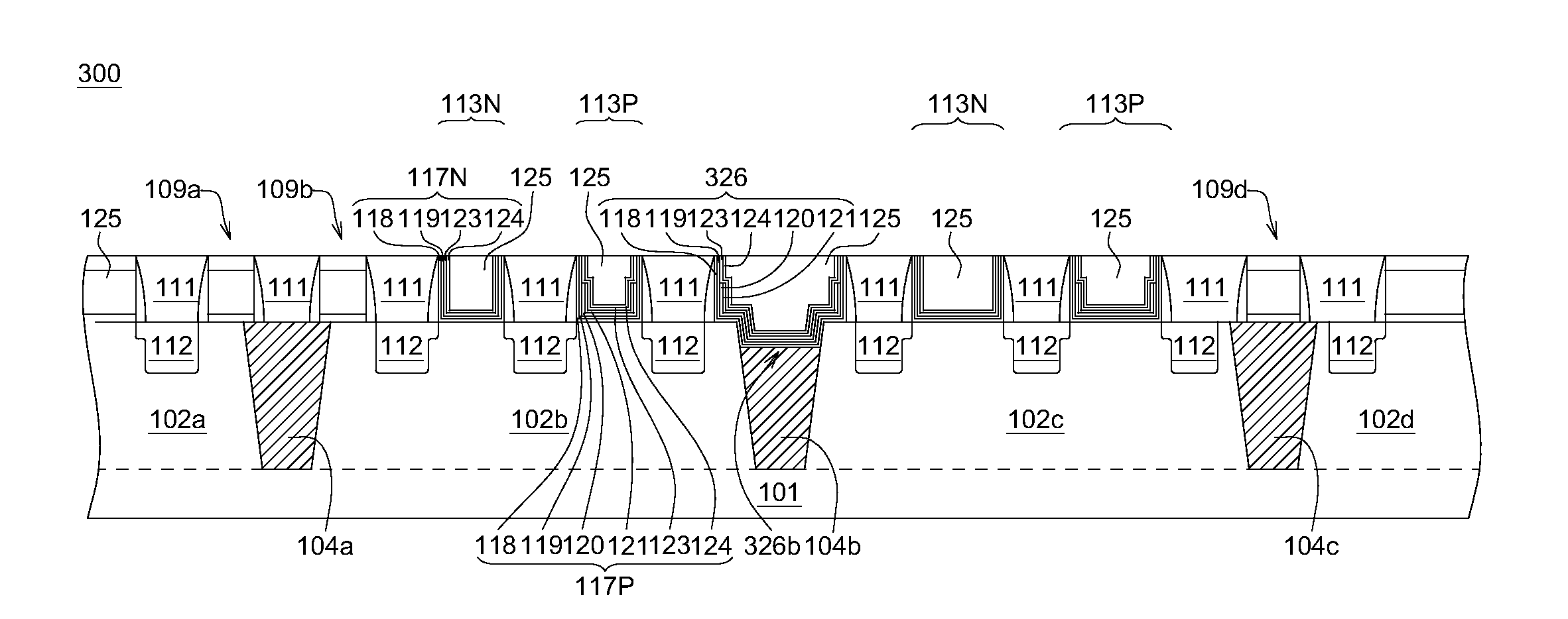
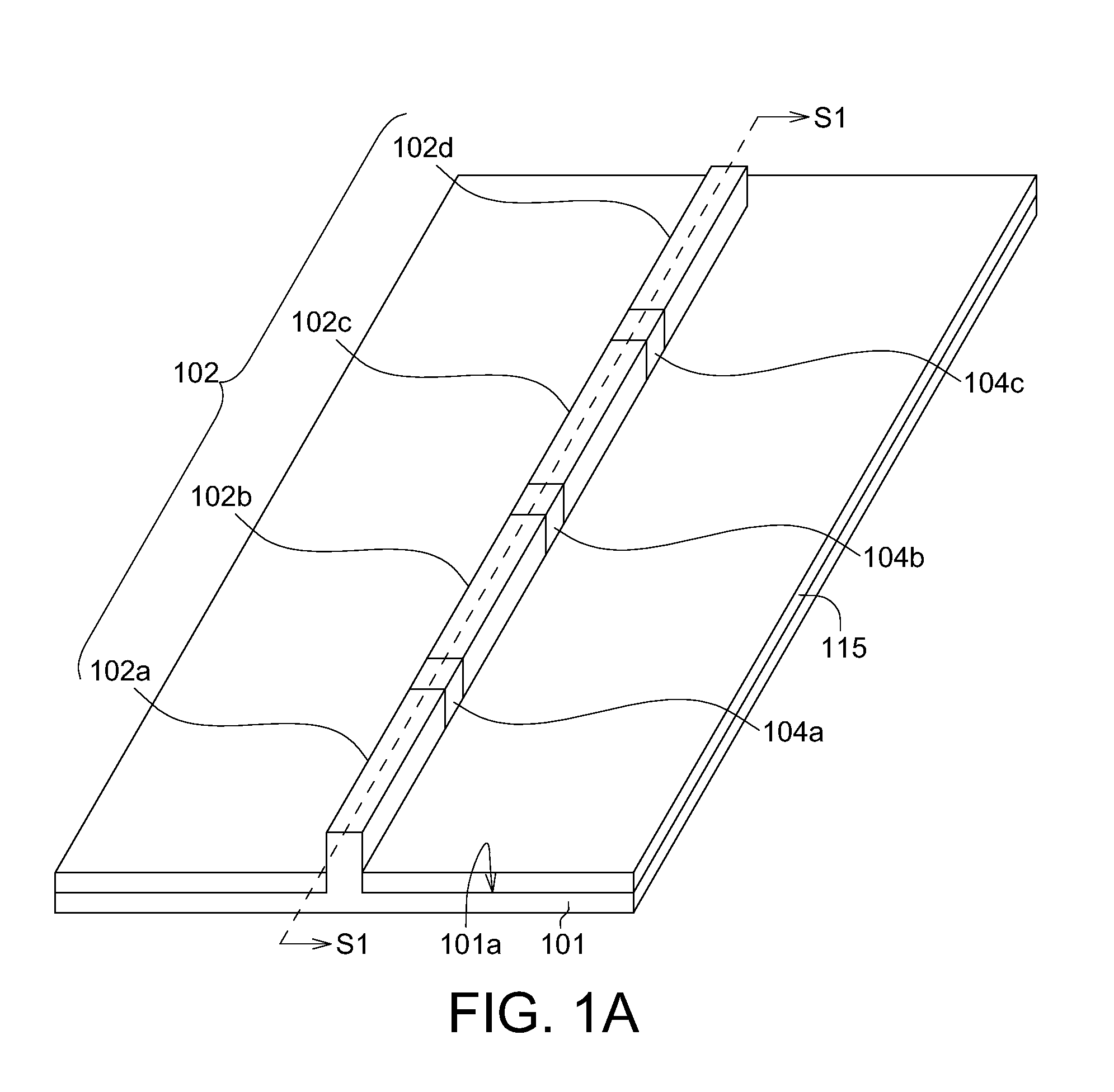
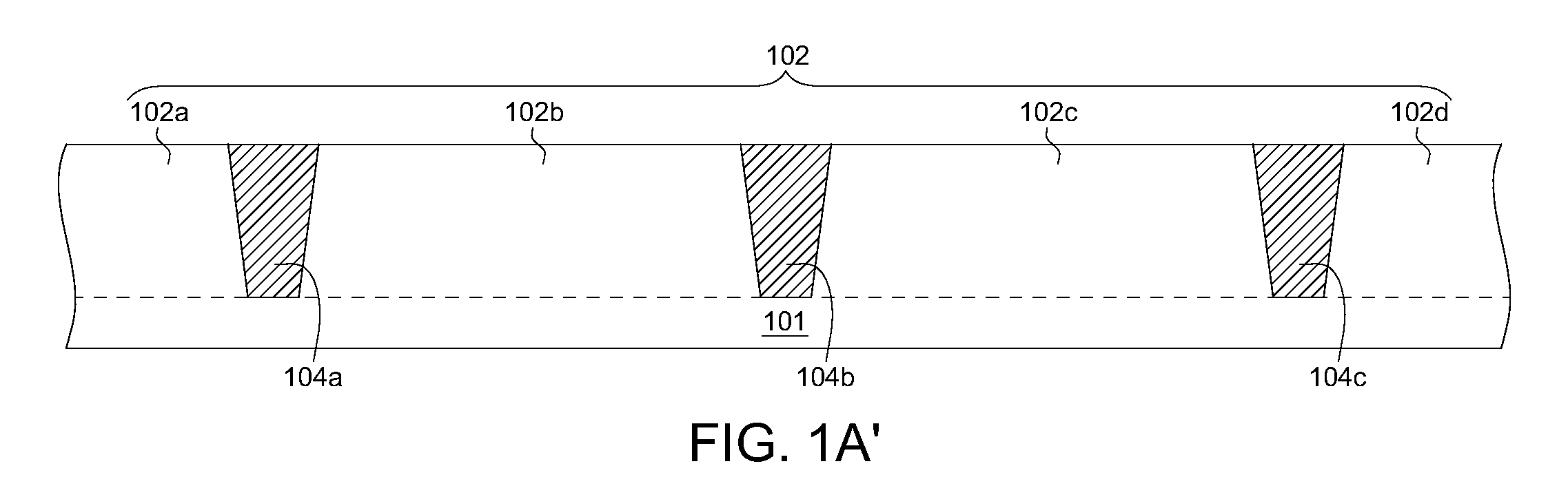
[0025]The embodiments as illustrated below provide a semiconductor device and method for fabricating the same. The present invention will now be described more specifically with reference to the following embodiments illustrating the method for fabricating a semiconductor integrated circuit (IC) 100 having at least one FinFET.

[0026]It is to be noted that the following descriptions of preferred embodiments of this invention are presented herein for purpose of illustration and description only. It is not intended to be exhaustive or to be limited to the precise form disclosed. Also, it is also important to point out that there may be other features, elements, steps and parameters for implementing the embodiments of the present disclosure which are not specifically illustrated. Thus, the specification and the drawings are to be regard as an illustrative sense rather than a restrictive sense. Various modifications and similar arrangements may be provided by the persons skilled in the ar...


PUM


Abstract

A semiconductor device comprises a substrate, a semiconductor fin, a first isolation structure and a first dummy structure. The semiconductor fin comprises a first sub-fin and a second sub-fin protruding from a surface of the substrate. The first isolation structure is disposed in the semiconductor fin used for electrically isolating the first sub-fin and the second sub-fin. The first dummy structure is disposed on the first isolation structure and laterally extends beyond the first isolation structure along a long axis of the semiconductor fin, so as to partially overlap a portion of the first sub-fin and a portion of the second sub-fin.

Description

[0001]This application claims the benefit of Taiwan application Serial No. 103134233, filed Oct. 1, 2014, the subject matter of which is incorporated herein by reference.BACKGROUND[0002]1. Technical Field[0003]The disclosure relates in generally related to a semiconductor device and method for fabricating the same, and more particularly to a device with a fin field-effect transistor (FinFET) and method for fabricating the same.[0004]2. Description of the Related Art[0005]As the evolution of semiconductor process, technology node has progressed into nanometer-scale phenomena, a semiconductor device with higher functional density is provided. However, the critical sizes and features dimension of the semiconductor device are simultaneously shrunk small enough to make it challenging to produce a semiconductor device with the advantages of higher functional density without deteriorating the device performance. For overcoming the challenge, a device with a three-dimension design, such as ...

Claims


Application Information

Patent Timeline
Patent Type & Authority Applications(United States)
IPC IPC(8): H01L21/8238H01L29/49H01L29/06H01L27/092H01L29/66
CPCH01L21/823821H01L27/092H01L29/66545H01L29/495H01L29/0653H01L29/4916H01L29/66795H01L21/823431H01L21/823456H01L21/823481H01L21/823842H01L21/823878H01L27/0886H01L27/0924H01L21/823814H01L29/0649H01L29/42364
Inventor TUNG, YU-CHENG
Owner UNITED MICROELECTRONICS CORP
Why Eureka
Try Eureka