

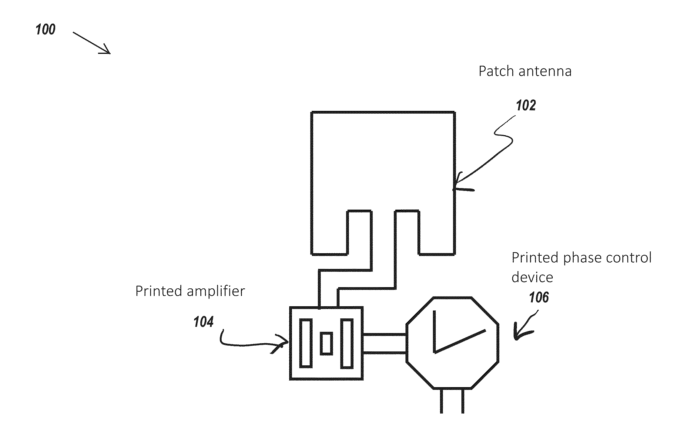
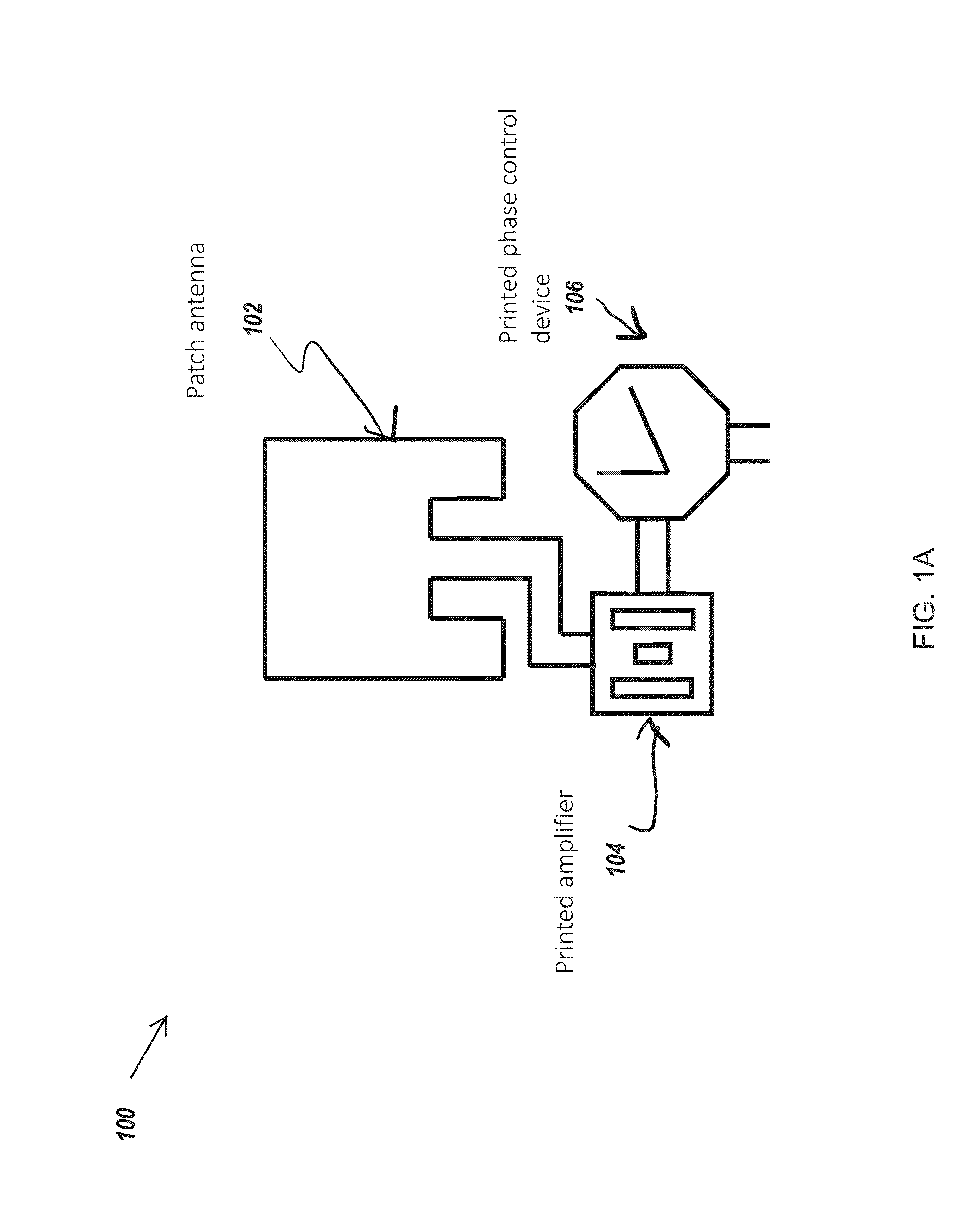
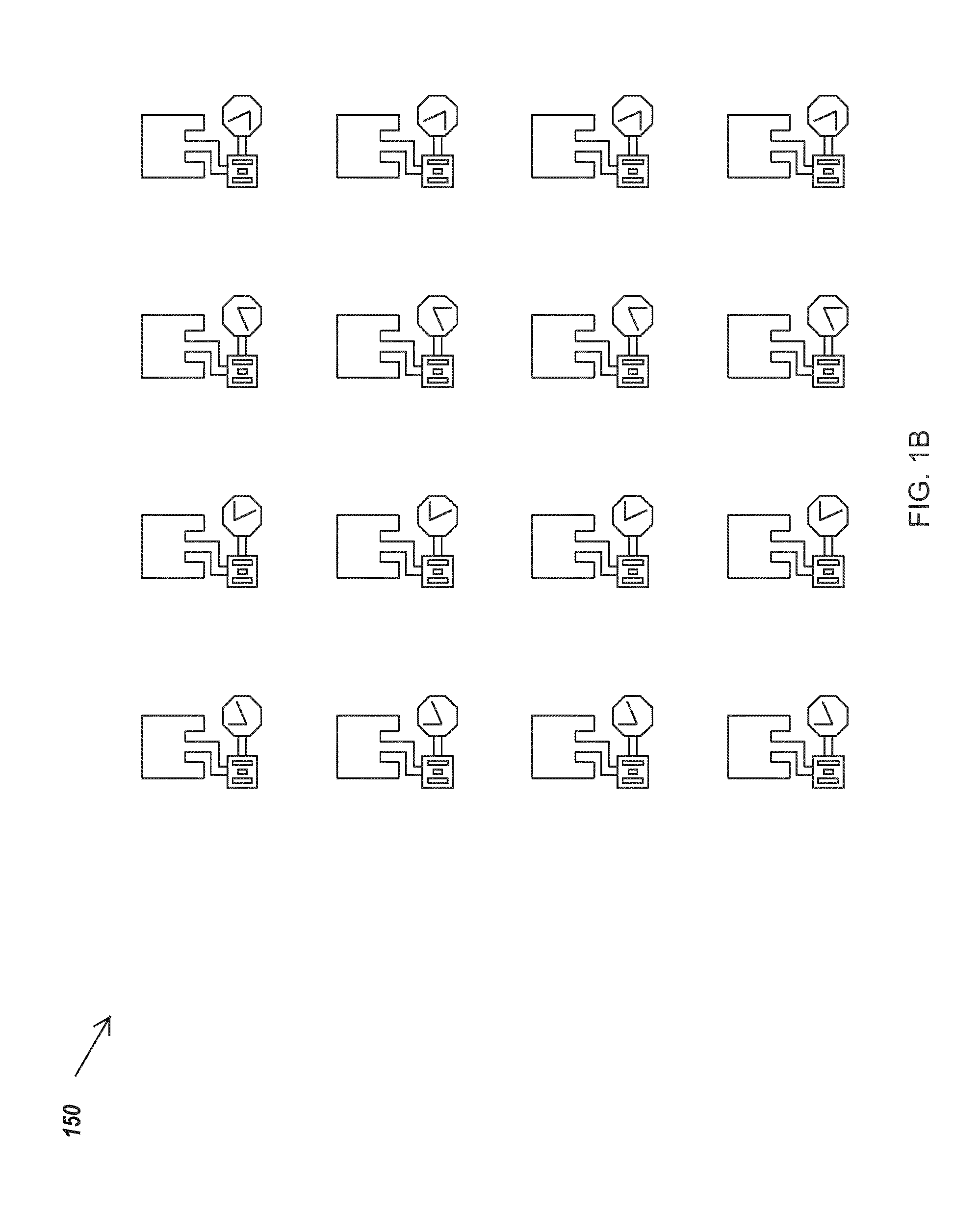
Micro assembled high frequency devices and arrays
a high-frequency device and array technology, applied in the field of micro-assembled, can solve the problems of increasing the size of the system and the cost of assembly, limiting the application of phased-array antenna systems, especially consumer products, and relatively few have been explored, so as to reduce the amount of non-active semiconductor area, and reduce the effect of cos
- Summary
- Abstract
- Description
- Claims
- Application Information
AI Technical Summary
Benefits of technology
Problems solved by technology
Method used
Image

Examples
Embodiment Construction
[0068]As used herein the expression “semiconductor element” and “semiconductor structure” are used synonymously and broadly refer to a semiconductor material, structure, device, or component of a device. Semiconductor elements include high-quality single crystalline and polycrystalline semiconductors, semiconductor materials fabricated via high-temperature processing, doped semiconductor materials, organic and inorganic semiconductors, and composite semiconductor materials and structures having one or more additional semiconductor components and / or non-semiconductor components, such as dielectric layers or materials and / or conducting layers or materials. Semiconductor elements include semiconductor devices and device components including, but not limited to, transistors, photovoltaics including solar cells, diodes, light-emitting diodes, lasers, p-n junctions, photodiodes, integrated circuits, and sensors. In addition, semiconductor element can refer to a part or portion that forms ...
PUM
| Property | Measurement | Unit |
|---|---|---|
| transparency | aaaaa | aaaaa |
| transparency | aaaaa | aaaaa |
| transparency | aaaaa | aaaaa |
Abstract
Description
Claims
Application Information