Optical detector and method for manufacturing the same

a technology of optical detectors and optical sensors, applied in the direction of sustainable manufacturing/processing, instruments, comonautical navigation instruments, etc., can solve the problems of complex driving electronics of generating pixels and displaying pixels, and achieve the effect of reducing the number of optical sensors

Active Publication Date: 2016-04-07
BASF AG
View PDF9 Cites 56 Cited by
  • Summary
  • Abstract
  • Description
  • Claims
  • Application Information

AI Technical Summary

Benefits of technology

[0076]Once the light propagation inside the detector, such as behind a lens of the detector, is modeled and / or recorded, this knowledge of light propagation provides a large number of advantages. This knowledge of light propagation, as an example, allows for slightly modifying the observer position after recording an image stack using image processing techniques. In a single image, an object may be hidden behind another object and is not visible. However, if the light scattered by the hidden object reaches the lens and through the lens one or more of the sensors, the object may be made visible, by changing the distance to the lens and / or the image plane relative to the optical axis, or even using non-planar image planes. The change of the observer position may be compared to looking at a hologram, in which changing the observer position slightly changes the image. The modification of observer position may be especially beneficial in motion capture and three dimensional video recordings as an unrealistically flat perception of three dimensional objects, known as cardboard effect, is avoided.
[0251]Thus, as an example, the second electrode may comprise one or more electrically conductive polymers, in combination with one or more layers of a metal. Preferably, the at least one electrically conductive polymer is a transparent electrically conductive polymer. This combination allows for providing very thin and, thus, transparent metal layers, by still providing sufficient electrical conductivity in order to render the second electrode both transparent and highly electrically conductive. Thus, as an example, the one or more metal layers, each or in combination, may have a thickness of less than 50 nm, preferably less than 40 nm or even less than 30 nm.

Problems solved by technology

A technically complex driving electronics of the generating pixels and the displaying pixels is required.

Method used


Image

  • Optical detector and method for manufacturing the same
  • Optical detector and method for manufacturing the same
  • Optical detector and method for manufacturing the same

Examples


embodiment 1

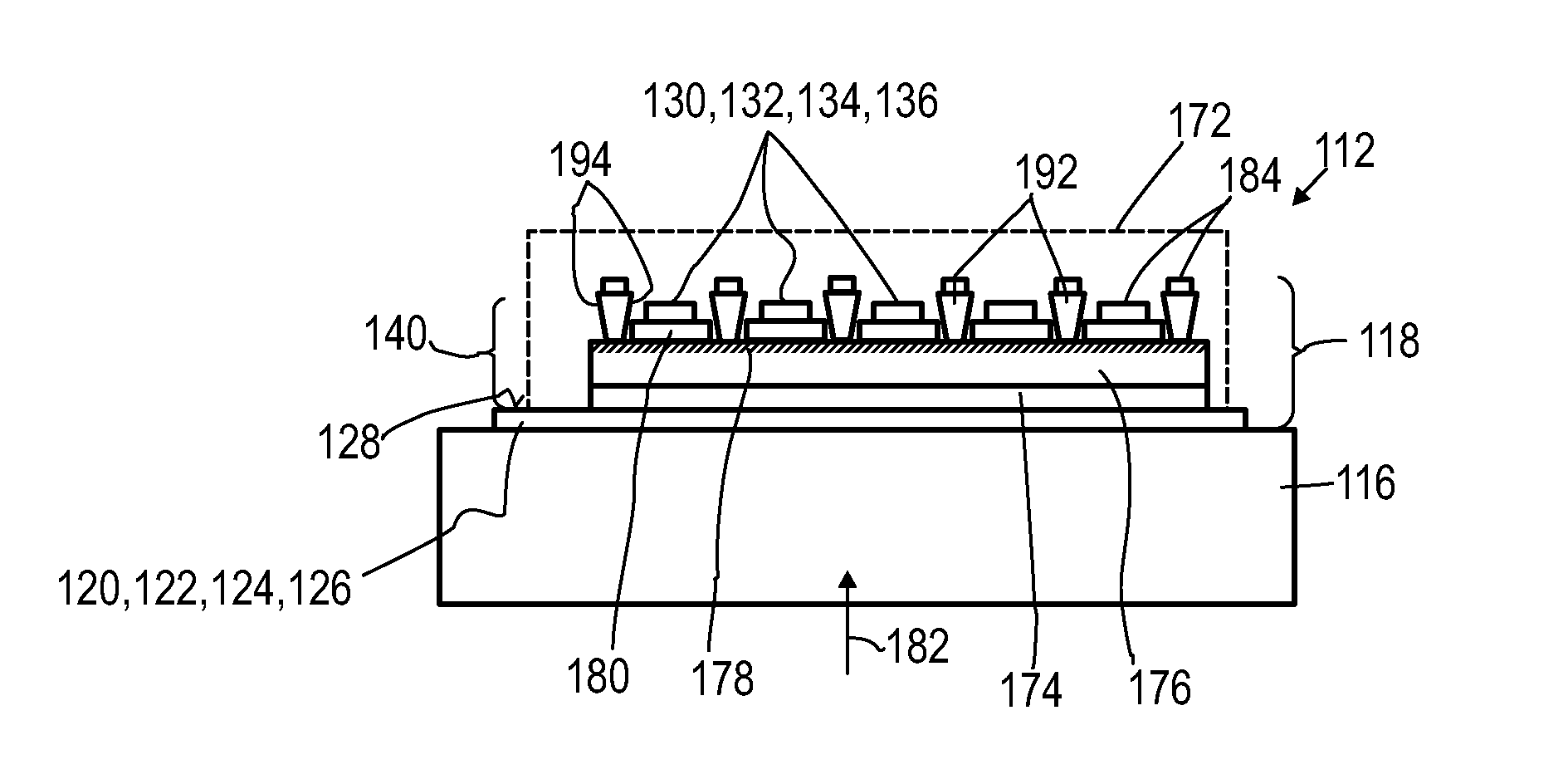
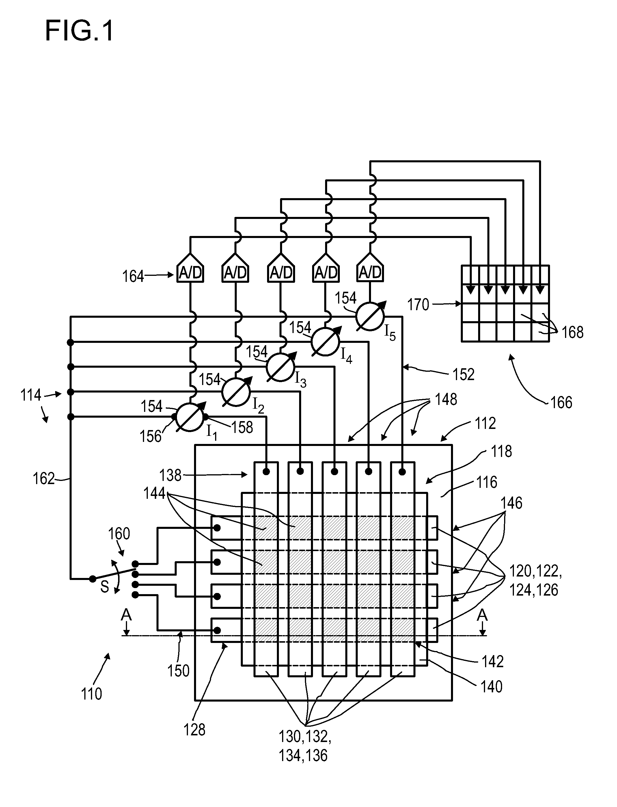
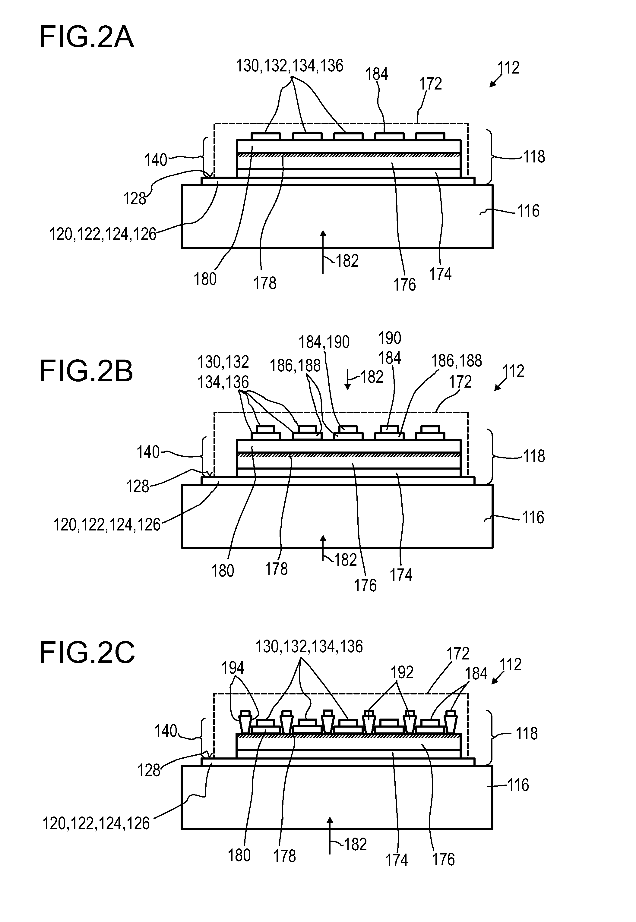
[0256]An optical detector, comprising:[0257]an optical sensor, having a substrate and at least one photosensitive layer setup disposed thereon, the photosensitive layer setup having at least one first electrode, at least one second electrode and at least one photovoltaic material sandwiched in between the first electrode and the second electrode, wherein the photovoltaic material comprises at least one organic material, wherein the first electrode comprises a plurality of first electrode stripes and wherein the second electrode comprises a plurality of second electrode stripes, wherein the first electrode stripes and the second electrode stripes intersect such that a matrix of pixels is formed at intersections of the first electrode stripes and the second electrode stripes; and[0258]at least one readout device, the readout device comprising a plurality of electrical measurement devices being connected to the second electrode stripes and a switching device for subsequently connecting...

embodiment 2

[0259]The optical detector according to the preceding embodiment, wherein the optical detector further comprises at least one optical element for optically imaging at least one object onto the optical sensor.

embodiment 3

[0260]The optical sensor according to the preceding embodiment, wherein the at least one optical element comprises at least one lens.


PUM


Abstract

An optical detector (110) is disclosed. The optical detector (110) comprises: —an optical sensor (112), having a substrate (116) and at least one photosensitive layer setup (118) disposed thereon, the photosensitive layer setup (118) having at least one first electrode (120), at least one second electrode (130) and at least one photovoltaic material (140) sandwiched in between the first electrode (120) and the second electrode (130), wherein the photovoltaic material (140) comprises at least one organic material, wherein the first electrode (120) comprises a plurality of first electrode stripes (124) and wherein the second electrode (130) comprises a plurality of second electrode stripes (134), wherein the first electrode stripes (124) and the second electrode stripes (134) intersect such that a matrix (142) of pixels (144) is formed at intersections of the first electrode stripes (124) and the second electrode stripes (134); and —at least one readout device (114), the readout device (114) comprising a plurality of electrical measurement devices (154) being connected to the second electrode stripes (134) and a switching device (160) for subsequently connecting the first electrode stripes (124) to the electrical measurement devices (154).

Description

FIELD OF THE INVENTION[0001]The present invention is based on previous European patent application number 13171898.3, the full content of which is herewith included by reference. The invention relates to an optical detector, a detector system, a human-machine interface, an entertainment device, a tracking system, a camera, a method for manufacturing an optical detector, a method of taking at least one image of an object and to various uses of the optical detector according to the present invention. The devices and methods according to the present invention are mainly used in the field of imaging and camera technology, such as for detecting at least one object and / or for taking an image of at least one object. Thus, the optical detector according to the present invention specifically may be used in the field of photography and / or for purposes of human-machine-interfaces or gaming. Other applications, however, are feasible.PRIOR ART[0002]A large number of optical sensors and photovolt...

Claims


Application Information

Patent Timeline
Patent Type & Authority Applications(United States)
IPC IPC(8): H01L51/44H04N5/225G01S17/06H01L51/42H01L27/30G01S17/86
CPCH01L51/441H01L51/4213H01L2031/0344G01S17/06H04N5/2254H01L27/307Y02E10/549Y02P70/50H04N25/70H04N25/75H10K19/202H10K39/32G01S17/86H04N25/71H04N25/76H10K30/81H10K30/10H10K30/82H10K30/151G01S17/08
Inventor BRUDER, INGMARSEND, ROBERTIRLE, STEPHANTHIEL, ERWIN
Owner BASF AG
Why Eureka
Try Eureka