Al technical title is built by PatSnap Al team. It summarizes the technical point description of the patent document.
a sensor device and direct magnetic field technology, applied in the direction of superconductive devices, magnetic field measurement using superconductive devices, instruments, etc., can solve the problem of poor spatial resolution (of several microns)
Inactive Publication Date: 2016-04-14
YEDA RES & DEV CO LTD
View PDF2 Cites 0 Cited by
Summary
Abstract
Description
Claims
Application Information
AI Technical Summary
This helps you quickly interpret patents by identifying the three key elements:
Problems solved by technology
Method used
Benefits of technology
Problems solved by technology
Scanning SQUID microscopy has the highest field sensitivity bu
Method used
Image
Click on the blue label to locate the original text in one second.
Reading with bidirectional positioning of images and text.
Examples
Embodiment Construction
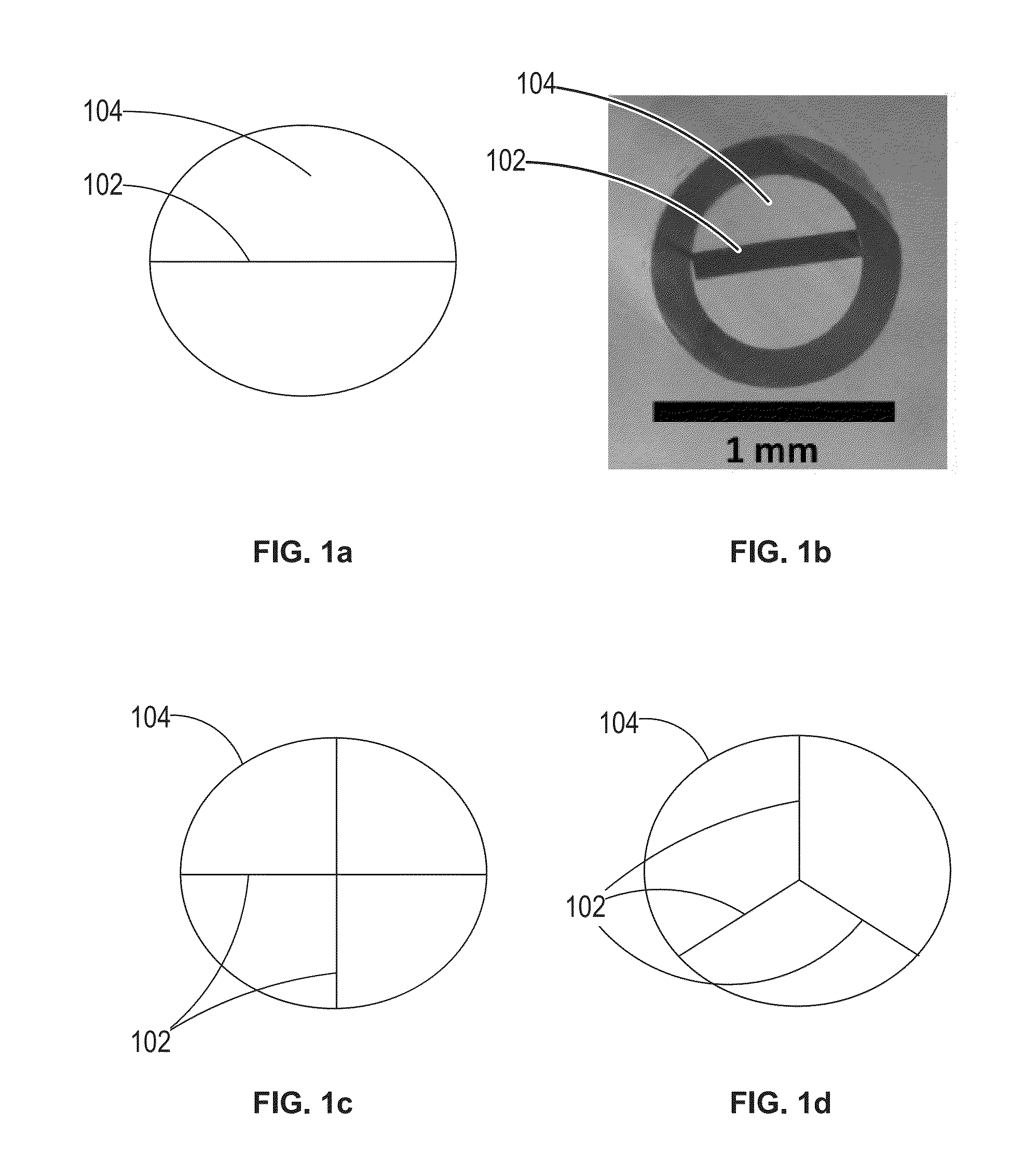
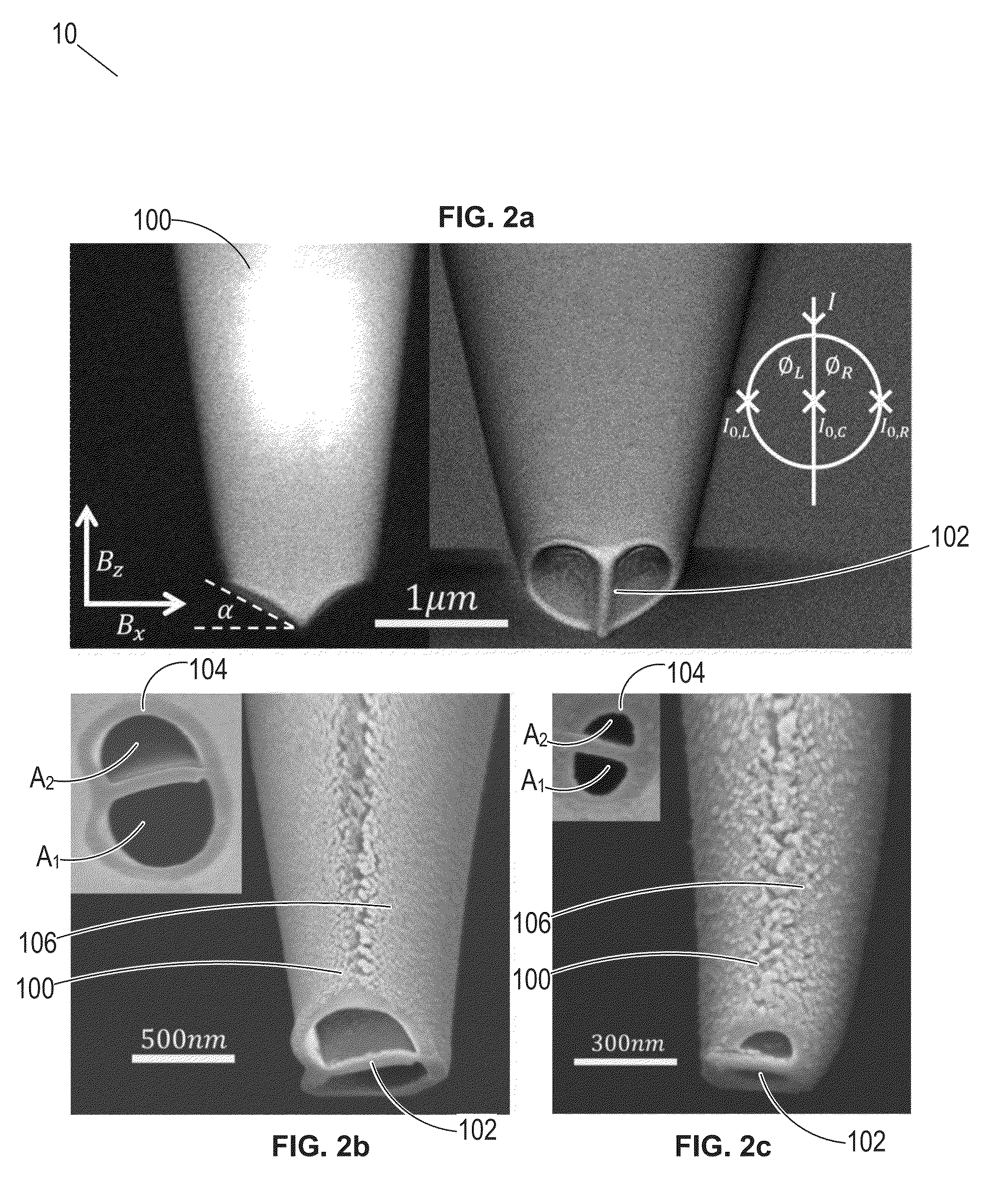
[0045]The present invention provides a sensor device comprising a probe carrying a three-dimensional magnetic field sensor. The probe has a conical tip portion with an edge being configured as the three-dimensional magnetic field sensor by which the probe, when in operation, directly approaches the surface of a sample. The sensor at the edge of the tip comprises at least three junctions, each junction being formed by a superconducting layer separated by a barrier. The barrier may be made of a non-superconducting material or may have defined regions of weaker superconductivity obtained by imposing geometrical constrictions. Reference is made to FIGS. 1a-1d showing specific and non-limiting examples of different possible cross sections of the tip of the three-dimensional sensor device having an edge with a closed-loop basis. The conical tip portion forms a structure having at least one arc-like part 102 crossing the opening of the tip portion such that the edge has a closed-loop basis...
PUM
Property
Measurement
Unit
Angle
aaaaa
aaaaa
Diameter
aaaaa
aaaaa
Magnetic field
aaaaa
aaaaa
Abstract
The present invention discloses a sensor device comprising a probe carrying a three-dimensional magnetic field sensor. The probe has a conical tip portion with an edge being configured as the three-dimensional magnetic field sensor. The sensor at the edge of the tip comprises at least three Josephson junctions, each junction being formed of a superconducting layer interrupted by a barrier. The barrier comprises a non-superconducting layer or a geometrical constriction. The conical tip portion of the probe forms a tapered three-dimensional structure having at least one arc-like part crossing the opening of the tip portion such that the apex has a closed-loop basis and a plurality of complimentary spaced-apart facets defined by the at least one arc, thereby enabling measurement of both in-plane and out-of-plane magnetic fields separately.
Description
TECHNOLOGICAL FIELD[0001]This invention relates to local magnetic field sensor devices for direct magnetic field vector imaging.REFERENCES[0002]References considered to be relevant as background to the presently disclosed subject matter are listed below:[0003][1] A. Finkler, Y. Segev, Y. Myasoedov, M. L. Rappaport, L. Ne'eman, D. Vasyukov, E. Zeldov, M. E. Huber, J. Martin, and A. Yacoby. Self-aligned nanoscale squid on a tip. Nano letters, 10(3):1046-1049, 2010.[0004][2] A. Finkler, D. Vasyukov, Y. Segev, L. Ne'eman, E O Lachman, M L Rappaport, Y. Myasoedov, E. Zeldov, and ME Huber. Scanning superconducting quantum interference device on a tip for magnetic imaging of nanoscale phenomena. Review of Scientific Instruments, 83(7):073702-073702, 2012.[0005][3] D. L. Tilbrook. Nanosquid sensitivity for isolated dipoles and small spin populations. Superconductor Science and Technology, 22(6):064003, 2009.[0006][4] E. Zeldov, J. R. Clem, M. McElfresh, and M. Darwin. Magnetization and tran...
Claims
Application Information
Patent Timeline
Application Date:The date an application was filed.
Publication Date:The date a patent or application was officially published.
First Publication Date:The earliest publication date of a patent with the same application number.
Issue Date:Publication date of the patent grant document.
PCT Entry Date:The Entry date of PCT National Phase.
Estimated Expiry Date:The statutory expiry date of a patent right according to the Patent Law, and it is the longest term of protection that the patent right can achieve without the termination of the patent right due to other reasons(Term extension factor has been taken into account ).
Invalid Date:Actual expiry date is based on effective date or publication date of legal transaction data of invalid patent.
IPC IPC(8): G01R33/035G01R33/00
CPCG01R33/0052G01R33/0354G01R33/035
Inventor REINER, JONATHANEMBON, LIORANAHORY, YONATHANMYASOEDOV, YURIZELDOV, ELI