Supercharge Your Innovation With Domain-Expert AI Agents!

Systems and method for ohmic contacts in silicon carbide devices

a technology of silicon carbide and contacts, applied in semiconductor devices, semiconductor/solid-state device details, electrical devices, etc., can solve problems such as poor adhesion, damage to the device, and deformation of the resulting device structur

Active Publication Date: 2016-04-28
GENERAL ELECTRIC CO
View PDF9 Cites 1 Cited by
  • Summary
  • Abstract
  • Description
  • Claims
  • Application Information

AI Technical Summary

Benefits of technology

This approach facilitates the formation of reliable, low-resistance ohmic contacts in silicon carbide devices, improving contact resistivity and device yield, and enabling higher device densities and improved manufacturing processes.

Problems solved by technology

Additionally, during the construction of these low-resistance contacts, certain semiconductor device manufacturing techniques (e.g., lift-off technique) may lead to defects in the resulting device structure (e.g., rough edges, stringers, torn contacts, undesired excess metal, poor adhesion, and / or other forms of damage to the device).
Furthermore, other device manufacturing techniques (e.g., self-aligning techniques), including methods that work well for constructing silicon devices, often do not prove to be effective for constructing silicon carbide devices.

Method used


Image

  • Systems and method for ohmic contacts in silicon carbide devices
  • Systems and method for ohmic contacts in silicon carbide devices
  • Systems and method for ohmic contacts in silicon carbide devices

Examples


Embodiment Construction

[0023]One or more specific embodiments of the present disclosure will be described below. In an effort to provide a concise description of these embodiments, all features of an actual implementation may not be described in the specification. It should be appreciated that in the development of any such actual implementation, as in any engineering or design project, numerous implementation-specific decisions must be made to achieve the developers' specific goals, such as compliance with system-related and business-related constraints, which may vary from one implementation to another. Moreover, it should be appreciated that such a development effort might be complex and time consuming, but would nevertheless be a routine undertaking of design, fabrication, and manufacture for those of ordinary skill having the benefit of this disclosure.

[0024]When introducing elements of various embodiments of the present disclosure, the articles “a,”“an,”“the,” and “said” are intended to mean that th...


PUM

PropertyMeasurementUnit
annealing temperatureaaaaaaaaaa

Abstract

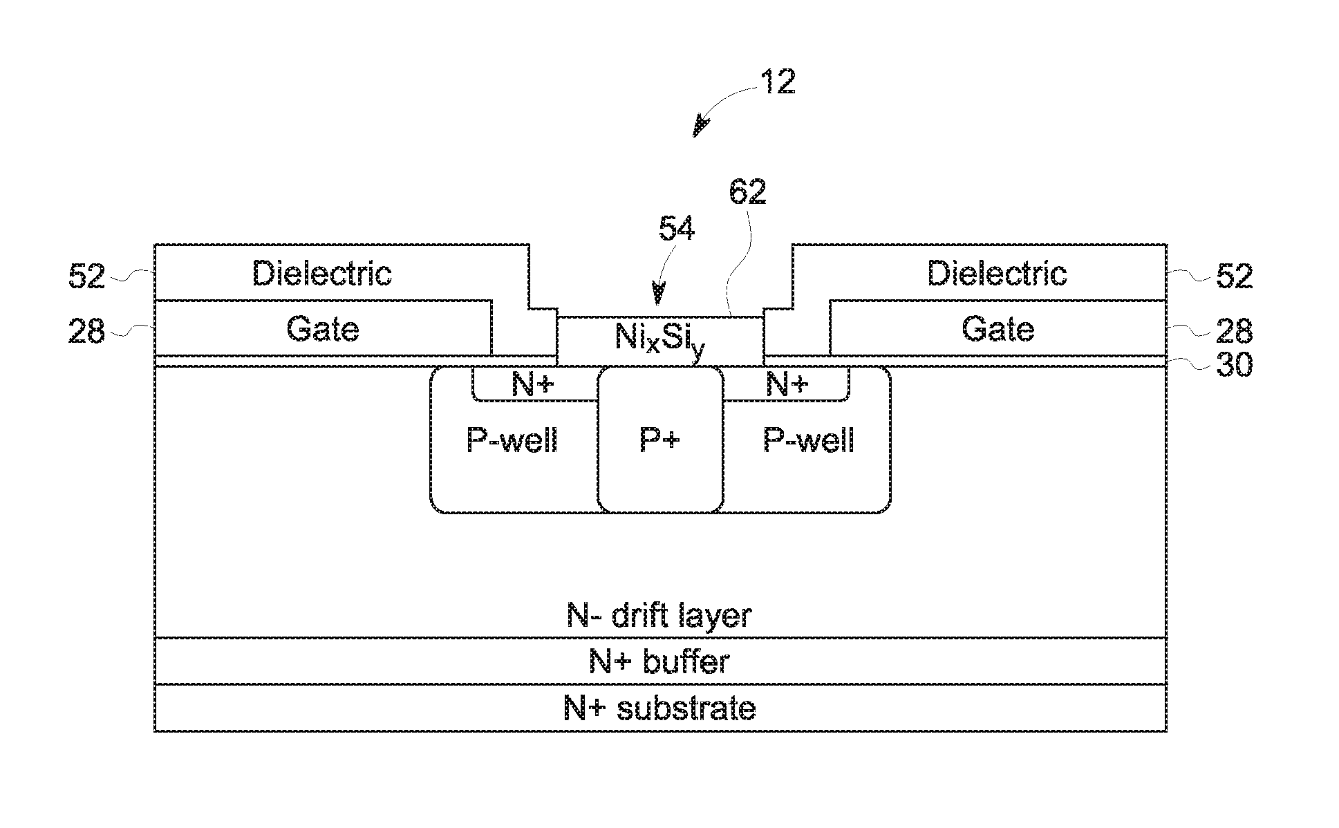
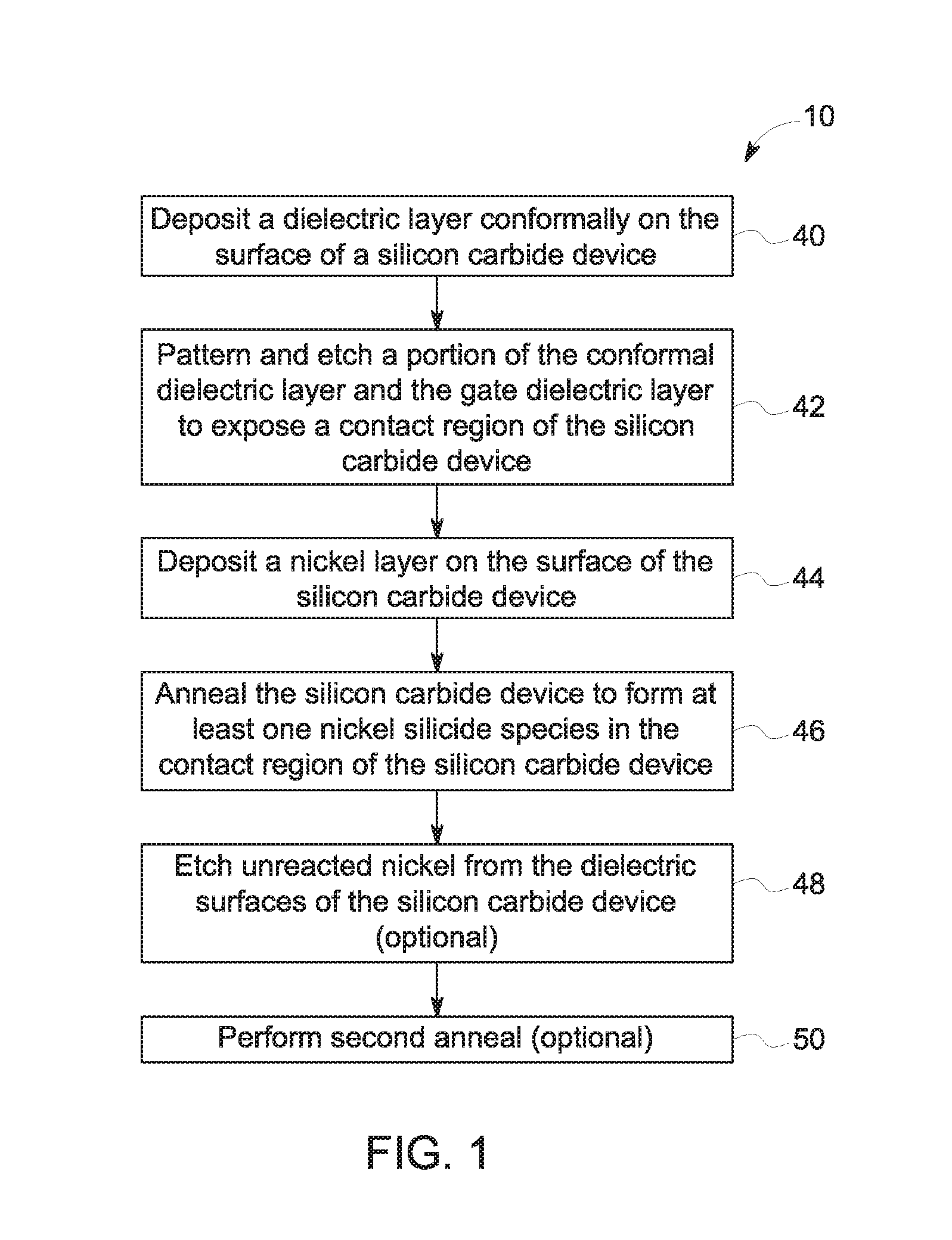
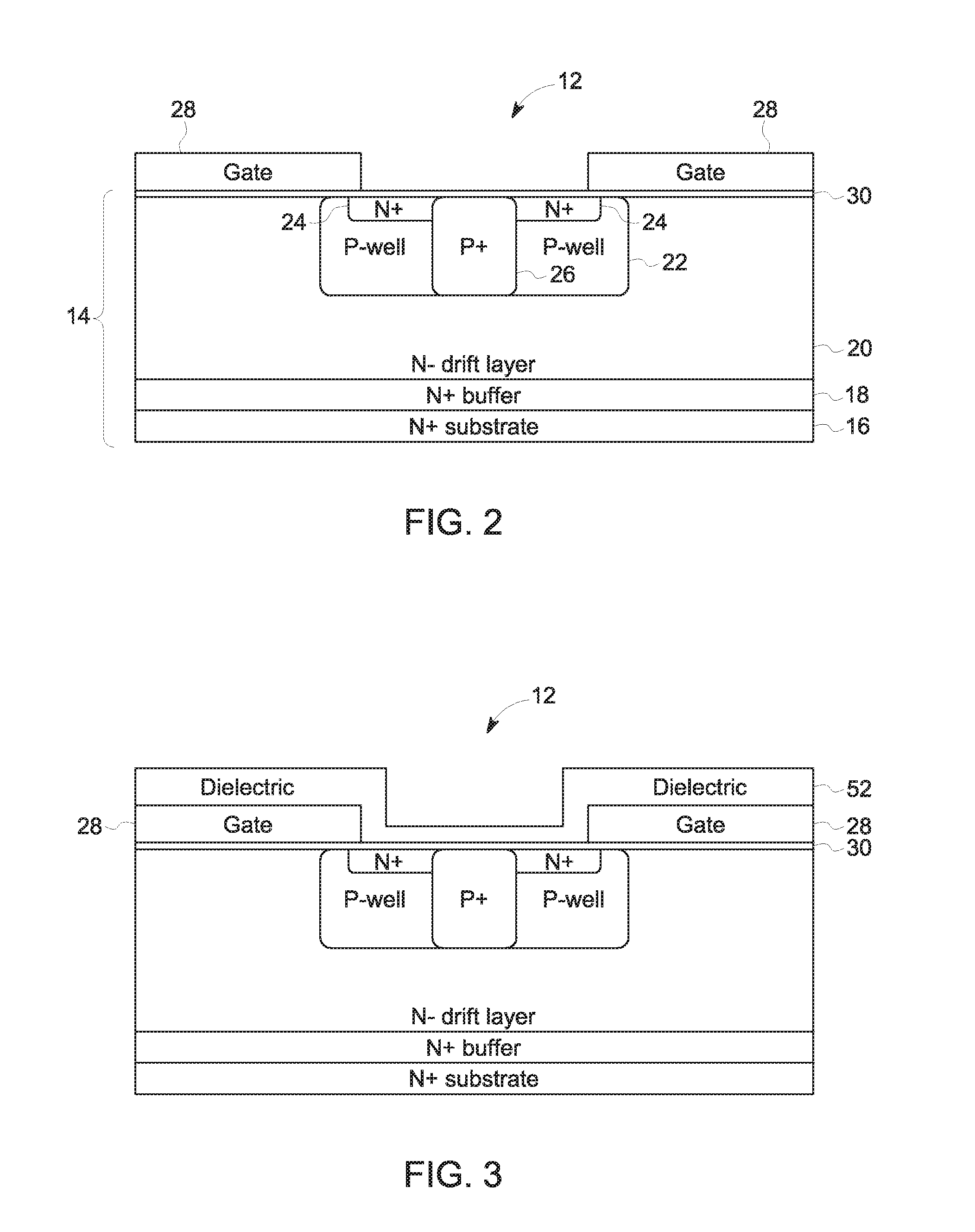
A silicon carbide device is presented that includes a gate electrode disposed over a portion of a silicon carbide substrate as well as a dielectric film disposed over the gate electrode. The device has a contact region disposed near the gate electrode and has a layer disposed over the dielectric film and over the contact region. The layer includes nickel in portions disposed over the dielectric film and includes nickel silicide in portions disposed over the contact region. The nickel silicide layer is configured to provide an ohmic contact to the contact region of the silicon carbide device.

Description

BACKGROUND[0001]The subject matter disclosed herein relates to silicon carbide semiconductor devices and, more specifically, to silicon carbide semiconductor devices for power applications.[0002]During fabrication of a semiconductor device, such as a field-effect transistor (FET), one or more contacts may be formed (e.g., in a contact region of a FET device). In general, it may be desirable for a contact to have a low resistance (e.g., an ohmic contact) when constructing, for example, a contact via in a silicon carbide FET device. Additionally, during the construction of these low-resistance contacts, certain semiconductor device manufacturing techniques (e.g., lift-off technique) may lead to defects in the resulting device structure (e.g., rough edges, stringers, torn contacts, undesired excess metal, poor adhesion, and / or other forms of damage to the device). Furthermore, other device manufacturing techniques (e.g., self-aligning techniques), including methods that work well for c...

Claims


Application Information

Patent Timeline
Patent Type & Authority Applications(United States)
IPC IPC(8): H01L21/04H01L29/78H01L29/808H01L29/45H01L21/3213H01L21/285H01L29/66H01L21/324H01L21/31H01L21/311H01L29/16H01L23/522
CPCH01L21/32133H01L21/31111H01L29/1608H01L29/7816H01L29/808H01L29/45H01L23/5226H01L21/28518H01L29/66068H01L29/66681H01L21/28568H01L21/28562H01L21/324H01L21/31H01L21/0485H01L29/66689H01L29/7802H01L2924/0002H01L2924/00H01L21/02697
Inventor STUM, ZACHARY MATTHEWGHANDI, REZA
Owner GENERAL ELECTRIC CO
Features
  • R&D
  • Intellectual Property
  • Life Sciences
  • Materials
  • Tech Scout
  • Unparalleled Data Quality
  • Higher Quality Content
  • 60% Fewer Hallucinations
Learn More