Data storage system

a data storage and data technology, applied in the field of data storage systems, can solve the problems of not working as a memory, reducing reliability, and restricting the erasing number of flash memory, so as to reduce the erasing time and reduce the exchange frequency

Inactive Publication Date: 2016-05-05
FANUC LTD
View PDF14 Cites 5 Cited by
  • Summary
  • Abstract
  • Description
  • Claims
  • Application Information

AI Technical Summary

Benefits of technology

[0015]The present invention, with the above configuration, enables to specify the task with many erasing time by storing the erasing time for each classification, and to decrease the erasing time by adjusting operation of the task, starting period of the task, and the like elongating the life time of the storage device and decreasing the exchange frequency.

Problems solved by technology

But the flash memory is restricted in erasing number for each block and reliability decreases as the erasing number increases, and finally does not work as a memory.
Generally, a storage device is designed securing enough erasing number based on operation of system and expected system life, since corruption of the stored data may cause a serious damage on the system.
However, the management of writing number and erasing number enables to prevent troubles at early stage by determining that the life time of the storage device ends and exchanging the storage device, but it is impossible to determine the reason of the increased writing number.

Method used


Image

  • Data storage system
  • Data storage system
  • Data storage system

Examples


first embodiment

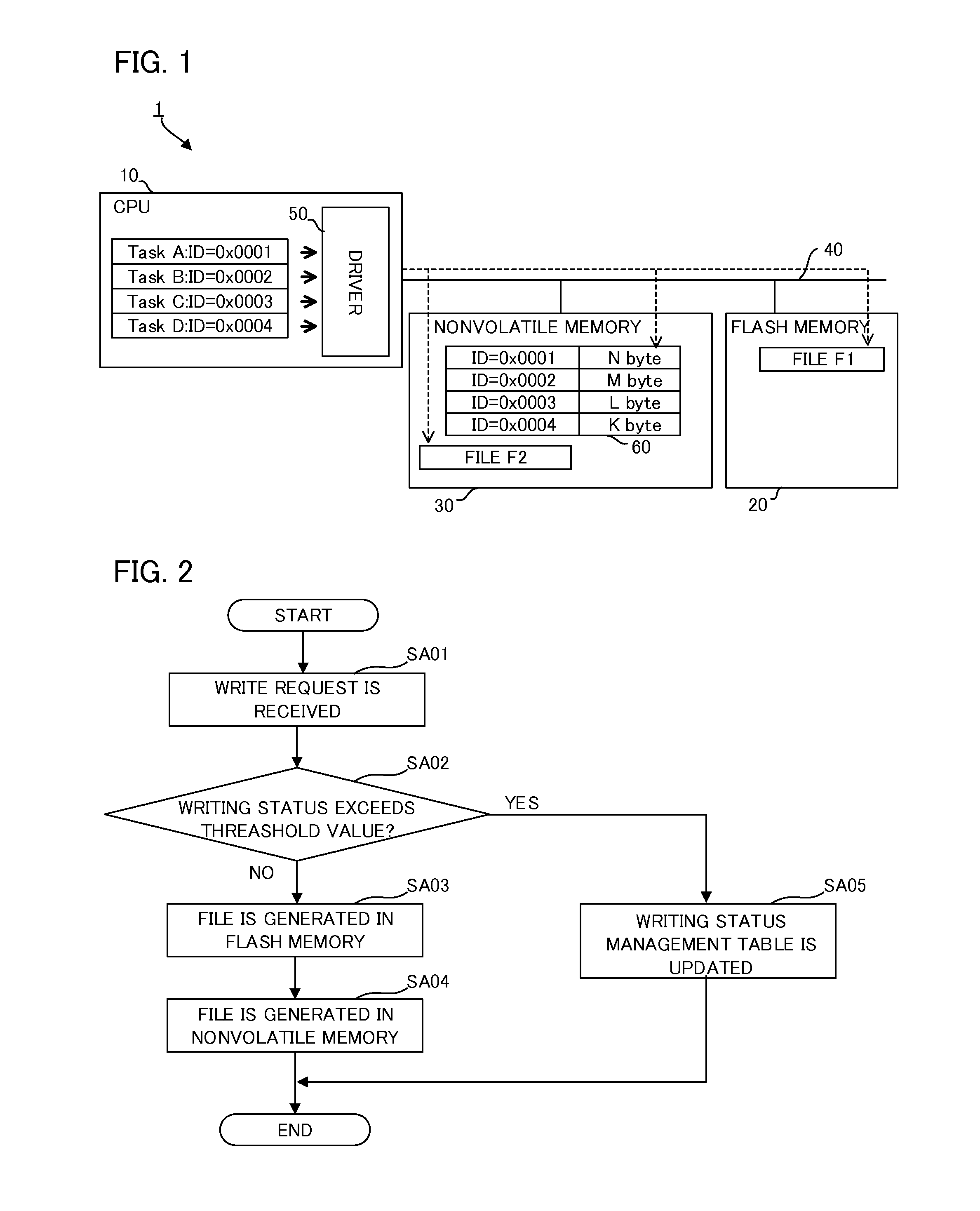
[0021]FIG. 1 is a functional block diagram of an electronic device according to the present invention. A data storage system in the present embodiment is configured as an electronic device in which CPU 10, a flash memory 20, and a nonvolatile memory 30 comprising an SRAM backed up by a battery and the like are connected to each other via a bus 40. Plural tasks are executed in time-division manner, and each task executes writing of a file in the flash memory 20. Task ID is assigned for each task by OS operating in the CPU 10, such that a driver 50 controlling writing of files can identify the tasks. Threshold is provided for each task in writing number, writing amount, and the like, preset in storage region for task management of OS in association with the task ID, and managed by the driver 50 by referring.

[0022]A writing status management table 60 storing the task ID in association with information of the writing status in the flash memory, is provided in the nonvolatile memory 30.

[...

second embodiment

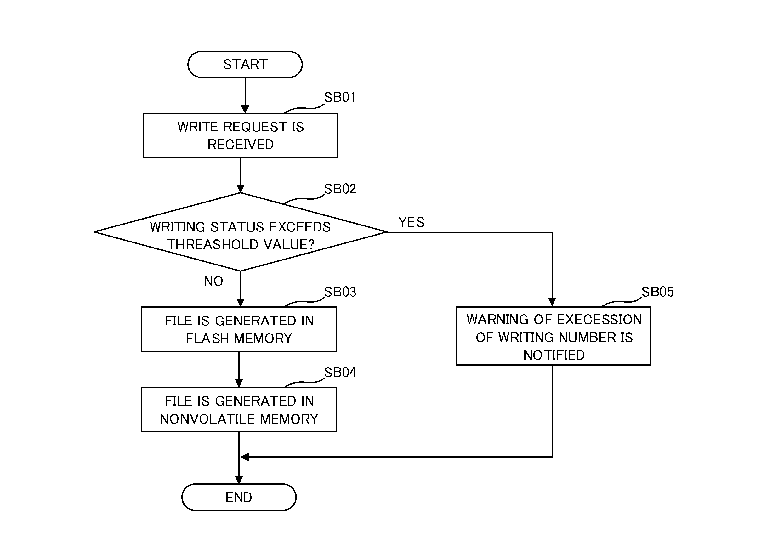
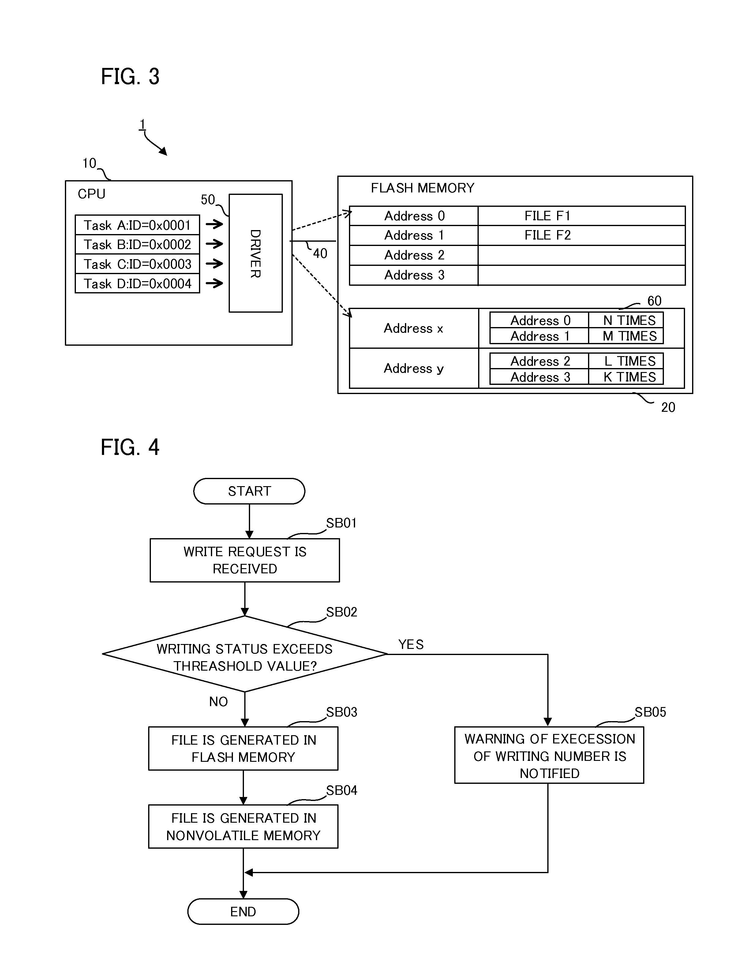
[0031]FIG. 3 is a schematic block diagram illustrating outline configuration of the data storage system according to the present invention. In the data storage system in the present embodiment, the CPU 10 and the flash memory 20 is connected to each other via the bus 40, and the wiring status management system 60 is provided in the flash memory 20.

[0032]In the CPU 10, plural tasks are executed in time-division manner, and each task executes wiring of a file in the flash memory 20.

[0033]Region in the flash memory is managed using logic address, and each task is configured to write in the region of each logic address different to each other. The writing status management table 60 provided in logic address Addressx in the flash memory stores information representing writing status in the region represented by the logic address, in association with the logic address to which each task executes writing. In FIG. 3, an example is shown in which information of writing number is stored as in...


PUM


Abstract

A data storage system including a processor configured to execute a plurality of tasks, wherein the processor is configured to generate writing status information based on the data relevant information and otre the data relevant information and the writing status information in association with each other in the nonvolatile memory when the processor write data in the recording medium based on demand of the task and writing to the recording medium is configured to be controlled based on the data relevant information and the write-in status information stored in nonvolatile memory.

Description

BACKGROUND OF THE INVENTION[0001]1. Field of the Invention[0002]The present invention relates to a data storage system, and more specifically to a data storage system which enables to investigate cause of writing / erasing number to a flash memory.[0003]2. Description of the Related Art[0004]NAND type flash memory is a nonvolatile memory which erasable in block unit. Storage device using the NAND type flash memory is widely used in a USB memory, an SD card, an SSD (Solid State Drive), and the like. But the flash memory is restricted in erasing number for each block and reliability decreases as the erasing number increases, and finally does not work as a memory.[0005]Generally, a storage device is designed securing enough erasing number based on operation of system and expected system life, since corruption of the stored data may cause a serious damage on the system. A case often happens in which number of writing exceeds the expected in the actual system operation, therefore a storage...

Claims


Application Information

Patent Timeline
Patent Type & Authority Applications(United States)
IPC IPC(8): G06F3/06
CPCG06F3/0653G06F3/0679G06F3/0614G06F3/0604G06F3/0616G06F3/064G06F12/0246G06F2212/1036G06F2212/7204
Inventor KOIZUMI, AKIRA
Owner FANUC LTD
Why Eureka
Try Eureka