Organic light emitting display device and fabricating method thereof

a technology of light-emitting display device and organic light-emitting diode, which is applied in the direction of solid-state devices, semiconductor devices, thermoelectric devices, etc., can solve the problems of black spot display of organic light-emitting diode or cathode electrode pixel damaged due to water, and water may remain in the planarization film,

Active Publication Date: 2016-05-12
LG DISPLAY CO LTD
View PDF4 Cites 23 Cited by
  • Summary
  • Abstract
  • Description
  • Claims
  • Application Information

AI Technical Summary

Benefits of technology

[0010]An object of the present invention is to provide an organic light emitting display device and a fabricating method thereof, in which an organic light emitting diode or a cathode electrode may be prevented from being damaged by outgassing generated due to water remaining in a planarization film.

Problems solved by technology

However, in spite of this effort, water may remain in the planarization film.
For example, if water of a minute amount of 150 ppm exists in the planarization film, the organic light emitting diode or the cathode electrode may be damaged by outgassing generated in the planarization film.
In this case, a problem may occur in that a pixel of the organic light emitting diode or the cathode electrode damaged due to water is displayed as a black spot.

Method used


Image

  • Organic light emitting display device and fabricating method thereof
  • Organic light emitting display device and fabricating method thereof
  • Organic light emitting display device and fabricating method thereof

Examples


Embodiment Construction

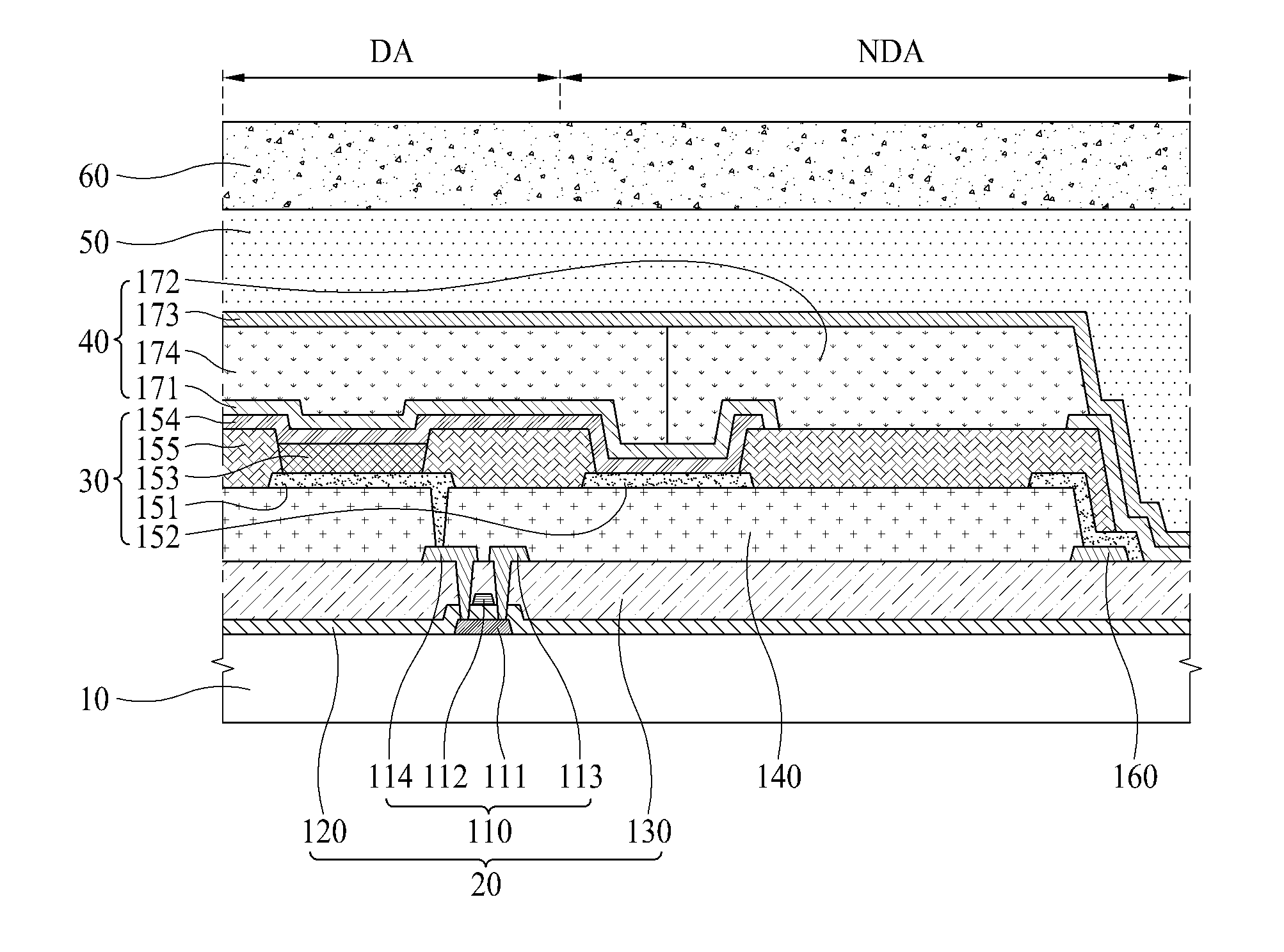
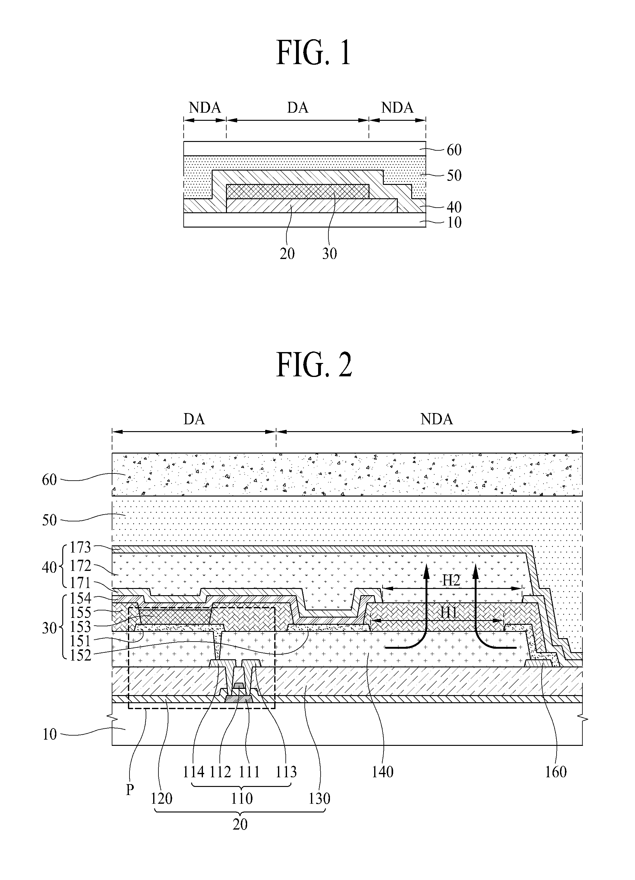
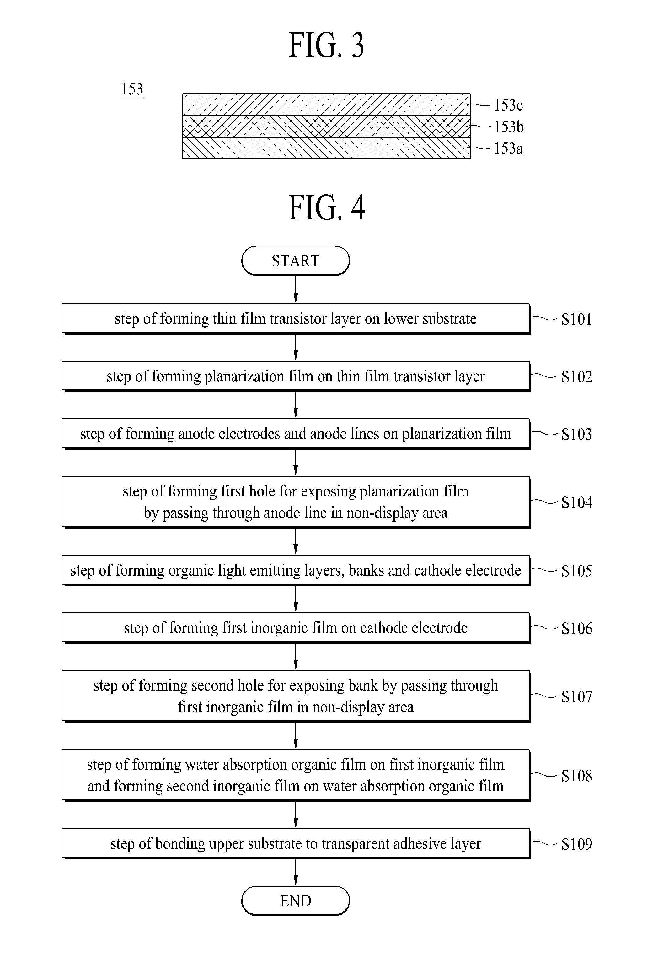
[0053]Reference will now be made in detail to the exemplary embodiments of the present invention, examples of which are illustrated in the accompanying drawings. Wherever possible, the same reference numbers will be used throughout the drawings to refer to the same or like parts. In the following description of the present invention, if detailed description of elements or functions known in respect of the present invention is determined to make the subject matter of the present invention unnecessarily obscure, the detailed description will be omitted. Also, titles of elements used in the following description may be selected considering easiness of drafting of the specification, and may be different from those of parts of the actual product.

[0054]FIG. 1 is an exemplary view briefly illustrating an organic light emitting display device according to an example embodiment of the present invention. In FIG. 1, one side sectional-view of an organic light emitting display device according ...


PUM

PropertyMeasurementUnit
DAaaaaaaaaaa
DAaaaaaaaaaa
DAaaaaaaaaaa

Abstract

An organic light emitting display device and a fabricating method thereof are disclosed, in which an organic light emitting diode or a cathode electrode may be prevented from being damaged by outgassing generated due to water remaining in a planarization film. The organic light emitting display device includes a substrate; a thin film transistor layer provided on the lower substrate; a planarization film provided on the thin film transistor layer to planarize the thin film transistor layer; an anode line provided on the planarization film to partially expose the planarization film in a non-display area corresponding to a periphery area of a display area; and a water absorption organic film provided on the exposed portion of the planarization film to at least partially absorb outgassing from the planarization film.

Description

CROSS REFERENCE TO RELATED APPLICATIONS[0001]This application claims the benefit of the Korean Patent Application No. 10-2014-0154512 filed on Nov. 7, 2014, which is hereby incorporated by reference for all purposes as if fully set forth herein.BACKGROUND OF THE INVENTION[0002]1. Field of the Invention[0003]The present invention relates to an organic light emitting display device and a fabricating method thereof.[0004]2. Discussion of the Related Art[0005]With the advancement of information society, a demand for a display device for displaying an image has increased in various forms. Recently, various flat panel display devices such as a liquid crystal display (LCD), a plasma display panel (PDP), and an organic light emitting display device have been used.[0006]Of the display devices, the organic light emitting display device which is a self light emitting display device is more excellent for a viewing angle, a contrast ratio, etc. than the LCD, and may be fabricated at a lightweigh...

Claims


Application Information

Patent Timeline
Patent Type & Authority Applications(United States)
IPC IPC(8): H01L51/52H01L51/00H01L27/32
CPCH01L51/5259H01L27/3258H01L27/3246H01L27/3276H01L2227/323H01L51/004H01L51/0077H01L51/005H01L51/0053H01L51/0073H10K59/10H10K59/122H10K50/846
Inventor KIM, JONGKYUNGHASUMI, TARO
Owner LG DISPLAY CO LTD
Why Eureka
Try Eureka