Organic light-emitting device and method of fabricating the same

a light-emitting device and organic technology, applied in the direction of thermoelectric device junction materials, semiconductor devices, electrical apparatus, etc., can solve the problems of reliability problems, contrast degradation of organic light-emitting devices, etc., and achieve the effect of low refractive index and high absorption coefficien

Active Publication Date: 2016-05-12
SAMSUNG DISPLAY CO LTD
View PDF8 Cites 47 Cited by
  • Summary
  • Abstract
  • Description
  • Claims
  • Application Information

AI Technical Summary

Benefits of technology

[0008]According to one or more exemplary embodiments, there is provided an organic light-emitting device including: a substrate; an anode formed on the substrate; an organic layer formed on the anode and including an emission layer; a cathode formed on the organic layer; a...

Problems solved by technology

However, the organic light-emitting device may suffer from contrast degradation or problems in expressing black that are caused by metal electrodes and metal wires, which reflect light (e.g., external light) received from the outside.
In order to reduce...

Method used


Image

  • Organic light-emitting device and method of fabricating the same
  • Organic light-emitting device and method of fabricating the same
  • Organic light-emitting device and method of fabricating the same

Examples


example 1

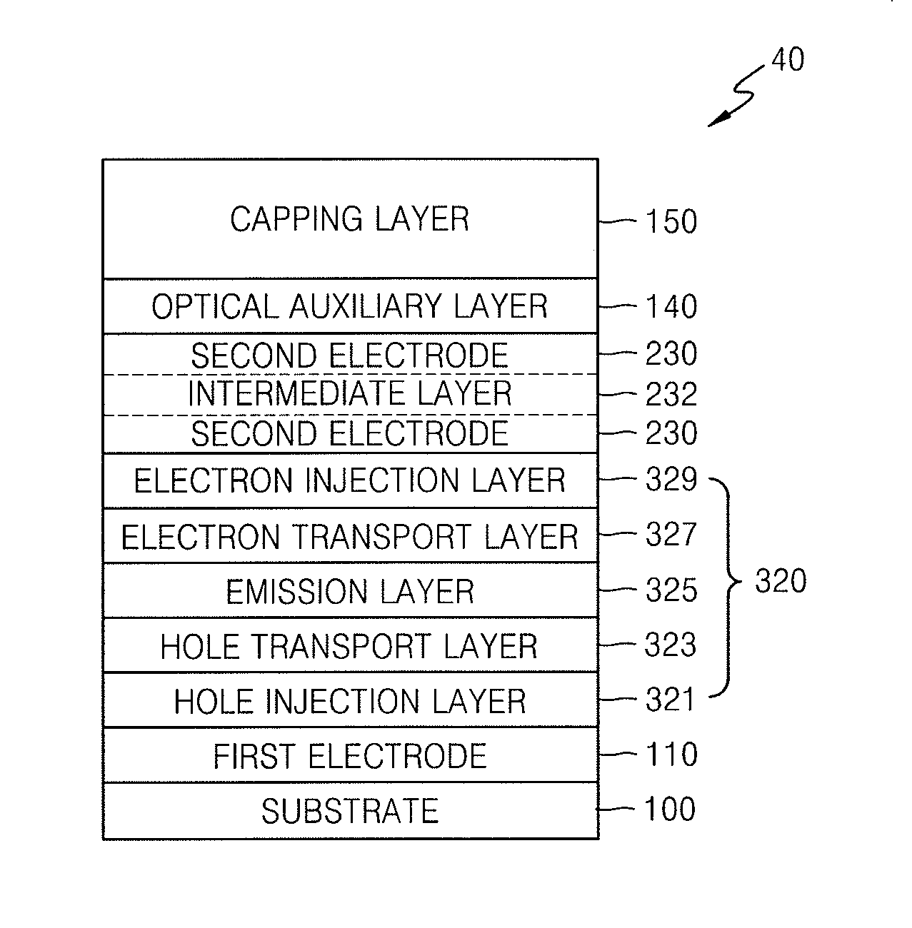
[0113]On top of low temperature polysilicon substrate (LTPS), an organic light-emitting device was fabricated in a stacked structure of ITO (7 nm) / HTL / EML / ETL / Yb (1.5 nm) / Ag:Mg (90:10 volume ratio, 10 volume % of Mg) (9 nm) / Yb (1 nm) / capping layer (85 nm).

example 2

Single Layer

[0125]Ag / ITO / HTL / EMUETUEIUcathode / Yb / CPL

example 3

Multiple Layer

[0126]Ag / ITO / HTL / EMUETL / EIL / cathode / Yb / CPL / Yb / CPL

[0127]CPL is a capping layer in Example 2 and Example 3.

[0128]FIG. 10 is a graph showing simulated efficiency of the organic light-emitting devices (blue diodes) of Examples 2 and 3 according to Y values of light emission color coordinate of the organic light-emitting devices. Here, the ranges of emission colors were limited to a blue region. When the Y value of color coordinate becomes high, blue wavelengths move toward long wavelengths, which corresponds that the thickness of the capping layer increases.

[0129]Referring to FIG. 10, the organic light-emitting device of Example 3 had better efficiency than that of the organic light-emitting device of Example 2 with respect to all the simulated wavelengths. That is, the organic light-emitting device having a structure of cathode / optical auxiliary layer (or intermediate layer) / cathode / optical auxiliary layer / capping layer was found to have higher efficiency than that of the...


PUM


Abstract

Provided is an organic light-emitting device including: a substrate; an anode on the substrate; an organic layer on the anode and including an emission layer; a cathode on the organic layer; an optical auxiliary layer on the cathode; and a capping layer on the optical auxiliary layer, wherein, in a visible light region, the optical auxiliary layer has a lower refractive index and a higher absorption coefficient as the capping layer.

Description

CROSS-REFERENCE TO RELATED APPLICATION[0001]Korean Patent Application No. 10-2014-0153734, filed on Nov. 6, 2014, in the Korean Intellectual Property Office, and entitled: “Organic Light-Emitting Device and Method of Fabricating the Same,” is incorporated by reference herein in its entirety.BACKGROUND[0002]1. Field[0003]One or more exemplary embodiments relate to an organic light-emitting device and a method of fabricating the same, and more particularly, to an organic light-emitting device capable of reducing reflection of external light and a method of fabricating the organic light-emitting device.[0004]2. Description of the Related Art[0005]An organic light-emitting device is a self-emission device that includes an anode, a cathode, and an organic light emission layer disposed between the anode and the cathode. Holes provided from the anode and electrons provided from the cathode recombine in the organic light emission layer and produce excitons. These excitons change from an exc...

Claims


Application Information

Patent Timeline
IPC IPC(8): H01L51/52
CPCH01L51/5281H01L51/5221H01L51/5092H01L51/5056H01L51/5072H01L51/5218H10K50/828H10K50/858H10K50/865H10K50/85H10K50/86H10K50/818
Inventor LEE, JAEYOUNGKIM, MYOUNGKIYOON, DAEYONGLIM, JAESUNGHWANG, JAEHOON
Owner SAMSUNG DISPLAY CO LTD
Why Eureka
Try Eureka