Semiconductor pixel unit for sensing near-infrared light, optionally simultaneously with visible light, and a semiconductor sensor comprising same

a semiconductor sensor and near-infrared light technology, applied in the field of semiconductor sensor, can solve the problems of inability to extract distance information from a single 2d image, requires two cameras and a powerful processor, and achieves the effect of a color sensor

Active Publication Date: 2016-06-09
MELEXIS TECH NV
View PDF37 Cites 41 Cited by
  • Summary
  • Abstract
  • Description
  • Claims
  • Application Information

AI Technical Summary

Benefits of technology

[0092]Color filters can be used to make the image sensor sensitive for particular colors, but the use of color filters are not essential for the present invention, because it is also possible to make a grayscale image sensor.
[0093]Preferably multiple color f...

Problems solved by technology

For machine vision applications, despite increasing resolution, increasing dynamic range of image sensors and increasing computational power of CPUs, it is impossible for a machine to extract distance information from a single 2D-image.
However, this requires two cameras and a powerful processor.
Although it is possible to get an image from a (pure) ti...

Method used


Image

  • Semiconductor pixel unit for sensing near-infrared light, optionally simultaneously with visible light, and a semiconductor sensor comprising same
  • Semiconductor pixel unit for sensing near-infrared light, optionally simultaneously with visible light, and a semiconductor sensor comprising same
  • Semiconductor pixel unit for sensing near-infrared light, optionally simultaneously with visible light, and a semiconductor sensor comprising same

Examples


Embodiment Construction

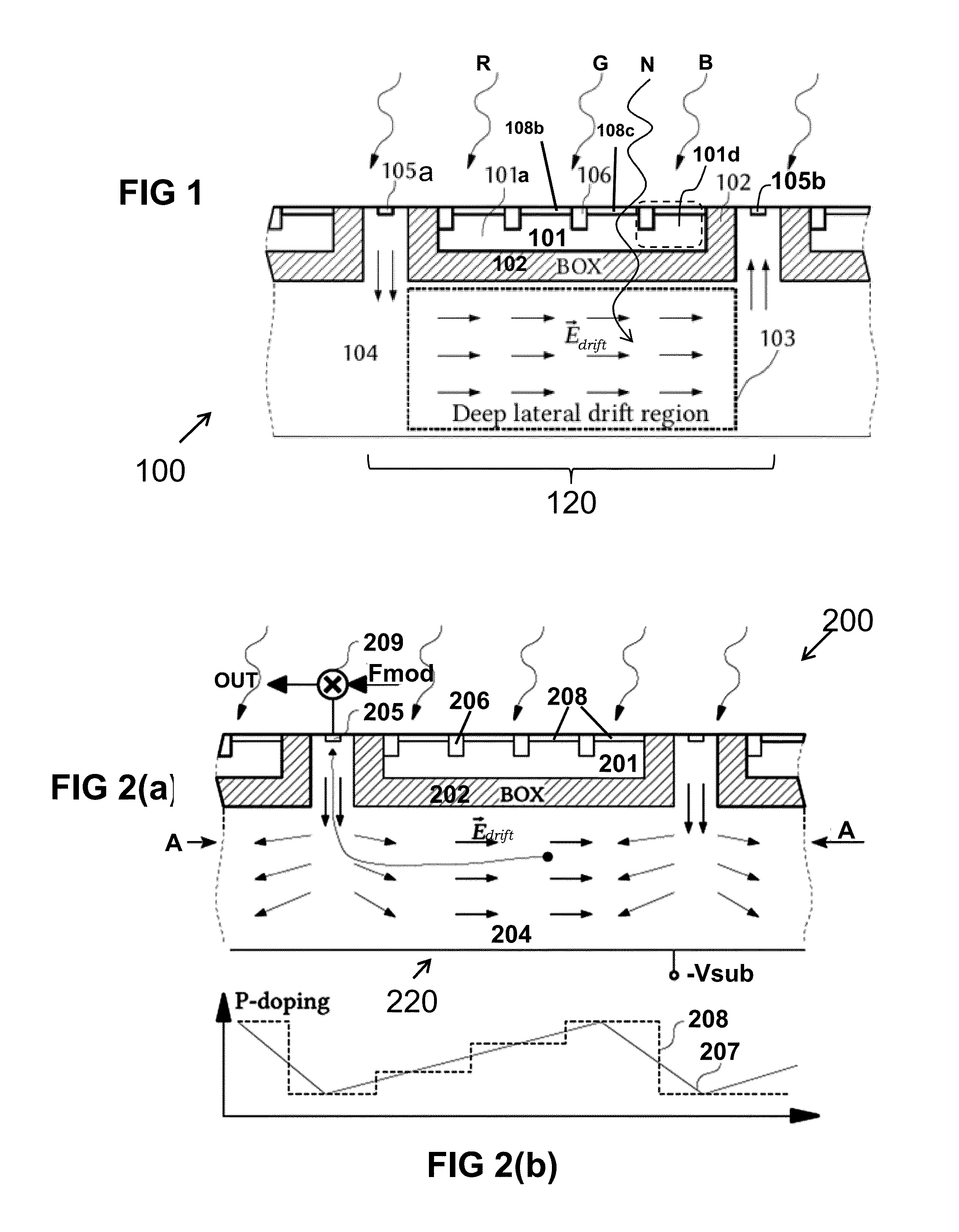
[0125]The present invention will be described with respect to particular embodiments and with reference to certain drawings but the invention is not limited thereto but only by the claims. The drawings described are only schematic and are non-limiting. In the drawings, the size of some of the elements may be exaggerated and not drawn on scale for illustrative purposes. The dimensions and the relative dimensions do not correspond to actual reductions to practice of the invention.

[0126]Furthermore, the terms first, second and the like in the description and in the claims, are used for distinguishing between similar elements and not necessarily for describing a sequence, either temporally, spatially, in ranking or in any other manner. It is to be understood that the terms so used are interchangeable under appropriate circumstances and that the embodiments of the invention described herein are capable of operation in other sequences than described or illustrated herein.

[0127]Moreover, t...


PUM


Abstract

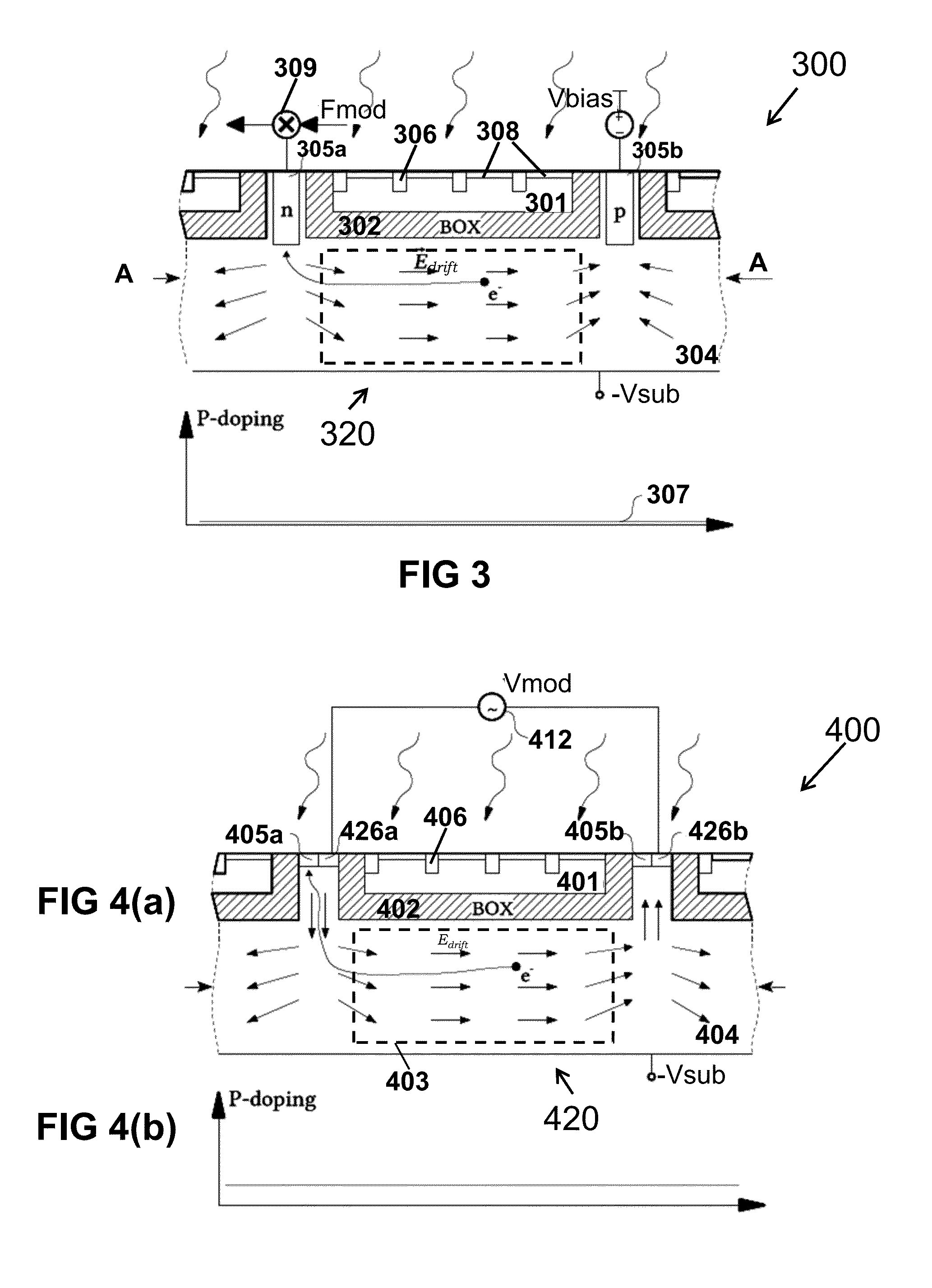
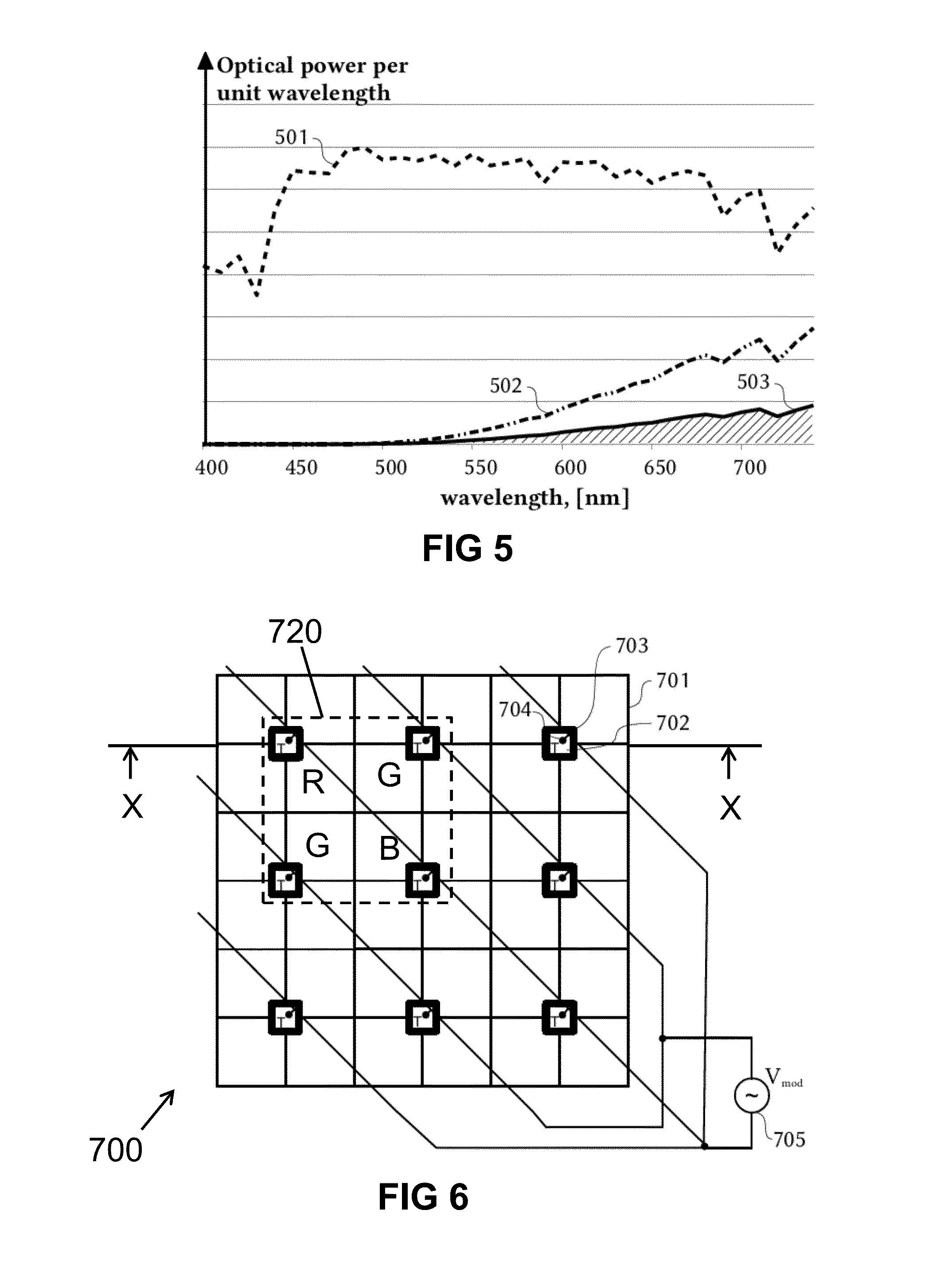
A semiconductor pixel unit for sensing near-infrared light, and for optionally simultaneously sensing visible light. The pixel unit comprises a single substrate with a first semiconductor region and a second semiconductor region electrically separated by an insulating region, for example a buried oxide layer. The pixel unit is adapted for generating a lateral electrical field in the second region for facilitating transport of photoelectrons generated in the second region by near-infrared light passing through the first region and the insulating region.

Description

FIELD OF THE INVENTION[0001]The invention relates to the field of semiconductor structures for near-infrared (NIR) light and optionally simultaneously sensing visible light. More in particular, the present invention relates to an imaging structure (e.g. a pixel unit) capable of simultaneously capturing visible light information (e.g. grayscale information or color information) and near-infrared light information (e.g. representative of distance information also known as “time-of-flight” (TOF) information).BACKGROUND OF THE INVENTION[0002]Solid state silicon image sensors became ubiquitous in the recent years. The first high quality image sensors were fabricated in a CCD technology which is nowadays being more and more replaced by CMOS technology. While typical CMOS based image sensor sensitivity is still lower than CCD based sensors, the integration advantages that CMOS technology can provide make it a technology of choice for today's image sensors. Besides the integration, CMOS tec...

Claims


Application Information

Patent Timeline
IPC IPC(8): G01S7/486G01S7/484G01S17/10G01S7/4863
CPCG01S7/4863G01S7/484G01S17/10H01L27/1461H01L27/1463H01L27/14645H01L27/14649
Inventor SELIUCHENKO, VOLODYMYR
Owner MELEXIS TECH NV
Why Eureka
Try Eureka