Selecting white point for OLED devices

a technology of organic light and diodes, which is applied in the direction of discharge tube luminescnet screens, other domestic articles, natural mineral layered products, etc., can solve the problems of improving power consumption relative to an rgb constructed of similar materials, and achieves effective initial white color, improved device efficiency, and reduced power consumption

Active Publication Date: 2008-04-24
GLOBAL OLED TECH
View PDF17 Cites 14 Cited by
  • Summary
  • Abstract
  • Description
  • Claims
  • Application Information

AI Technical Summary

Benefits of technology

[0012] It is an advantage of this invention that devices with effective initial white color (such as D65 white) can be obtained. It is an advantage of the present invention that it provides improved device efficiency, resulting in lower power consumption and longer lifetime. It is a further advantage for some embodiments of the present invention that such a device can be constructed using common OLED organic layers for all pixels, which does not require precision patterning of organic materials to form the pixels. Any device patterning necessary can be done as part of the formation of the active matrix components or passive matrix components by photolithographic methods, which are more precise methods than those commonly used to deposit organic layers. It is a further advantage for some embodiments of the present invention that an improved or extended color gamut is provided. This configuration permits for a four-pixel RGBW (red, green, blue, and white) configuration to be used in a bottom-emitting or top-emitting device, which further reduces the power consumption.
that it provides improved device efficiency, resulting in lower power consumption and longer lifetime. It is a further advantage for some embodiments of the present invention that such a device can be constructed using common OLED organic layers for all pixels, which does not require precision patterning of organic materials to form the pixels. Any device patterning necessary can be done as part of the formation of the active matrix components or passive matrix components by photolithographic methods, which are more precise methods than those commonly used to deposit organic layers. It is a further advantage for some embodiments of the present invention that an improved or extended color gamut is provided. This configuration permits for a four-pixel RGBW (red, green, blue, and white) configuration to be used in a bottom-emitting or top-emitting device, which further reduces the power consumption.

Problems solved by technology

This results in improved power consumption relative to an RGB constructed of similar OLED materials.

Method used


Image

  • Selecting white point for OLED devices
  • Selecting white point for OLED devices
  • Selecting white point for OLED devices

Examples


examples

[0166] The invention and its advantages can be better appreciated by the following inventive and comparative examples. In the following, mixed compositions are described in terms of percentages or ratios by volume, as are commonly used in the art.

examples 1 to 8

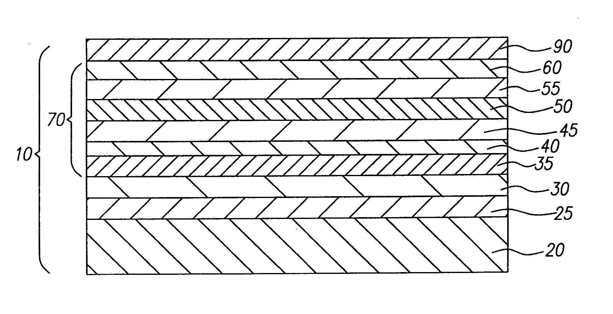
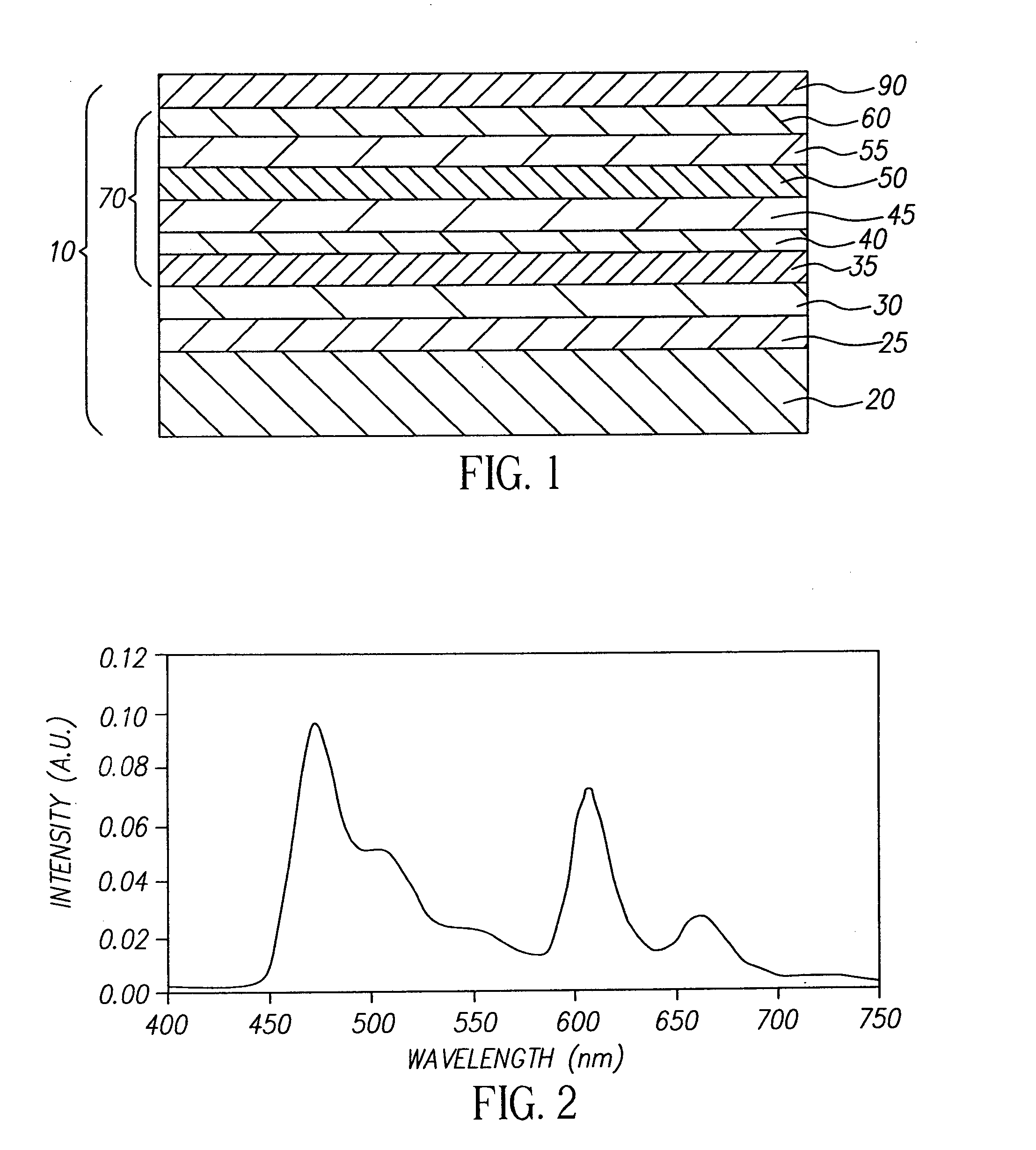
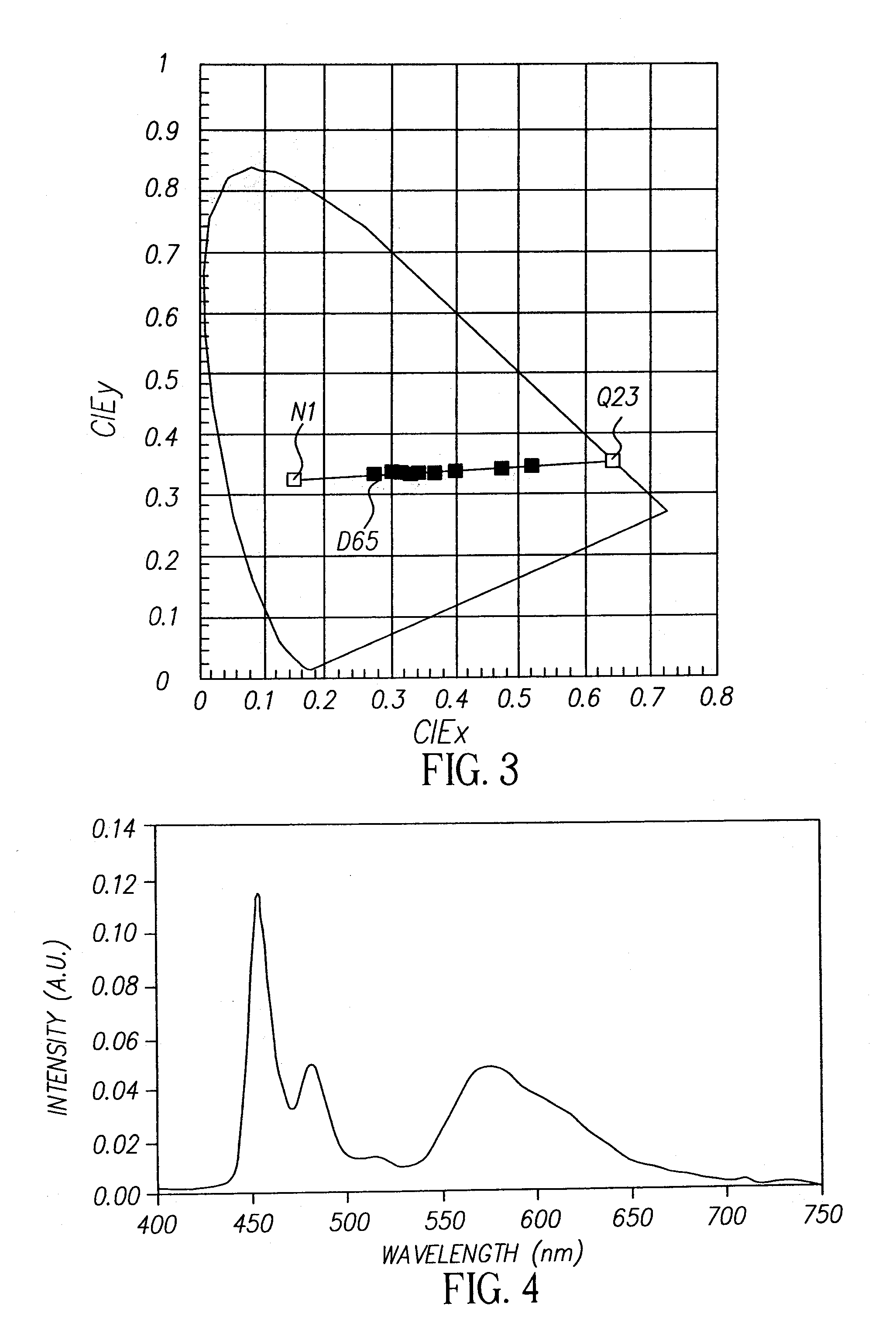
[0167] Examples 1 to 8 were prepared using a red-orange emitting layer using NPB host with Rubrene co-host and a red-orange dopant of Formula Q23. The blue-green emitting layer includes 9-(1-naphthyl)-10-(biphenyl-4-yl)anthracene (TBADN) host (as host) with 2.5% 4-(di-p-tolylamino)-4′-[(di-p-tolylamino)styryl]stilbene (Formula N1) (as dopant) and 6.4% NPB as co-dopant.

example 1

[0168] A comparative OLED device was constructed in the following manner:

[0169] 1. A clean glass substrate was vacuum-deposited with indium tin oxide (ITO) to form a transparent electrode of 85 nm thickness;

[0170] 2. The above-prepared ITO surface was treated with a plasma oxygen etch, followed by plasma deposition of a 0.5 nm layer of a fluorocarbon polymer (CFx) as described in U.S. Pat. No. 6,208,075;

[0171] 3. The above-prepared substrate was further treated by vacuum-depositing a 240 nm layer of 4,4′-bis[N-(1-naphthyl)-N-phenylamino]biphenyl (NPB) as a hole-transporting layer (HTL);

[0172] 4. A 28 nm layer of NPB (as host) with 28% Rubrene and 0.4% red-orange emitting dopant as shown in Formula Q23 were deposited on to the HTL layer to form a red-orange emitting first light-emitting layer;

[0173] 5. A coating of 47 nm of 9-(1-naphthyl)-10-(biphenyl-4-yl)anthracene (TBADN) host with 2.5% 4-(di-p-tolylamino)-4′-[(di-p-tolylamino)styryl]stilbene (Formula N1) (as dopant) and 6.4%...


PUM


Abstract

A method for selecting two different light-emitting materials for use in an OLED device, each of which produces different color light, which combine to produce white light. Each light emitting material has its own point on a chromaticity diagram, and the light-emitting materials are selected such that, when a line is drawn between the first point and the second point, it passes through a desired white area defined on a chromaticity diagram.

Description

CROSS REFERENCE TO RELATED APPLICATIONS [0001] This application is a divisional of pending U.S. patent application Ser. No. 10 / 990,865 filed Nov. 17, 2004 entitled “Selecting White Point for OLED Devices” by Jeffrey P. Spindler et al. [0002] Reference is made to commonly assigned U.S. patent application Ser. No. 10 / 780,436 filed Feb. 17, 2004 by Michele L. Ricks, et al., entitled “Anthracene Derivative Host Having Ranges of Dopants”, commonly assigned U.S. patent application Ser. No. 10 / 801,997 filed Mar. 16, 2004 by William J. Begley, et al., entitled “White Organic Light-Emitting Devices With Improved Performance”, commonly assigned U.S. patent application Ser. No. 10 / 838,665 filed May 4, 2004 by Tukaram K. Hatwar, et al., entitled “Improved Tuned Microcavity Color OLED Display”, and commonly assigned U.S. patent application Ser. No. 10 / 869,115 filed Jun. 16, 2004 by Michele L. Ricks, et al., entitled “Array of Light-Emitting OLED Microcavity Pixels”, the disclosures of which are ...

Claims


Application Information

Patent Timeline
Patent Type & Authority Applications(United States)
IPC IPC(8): H01L51/54
CPCH01L27/3213H01L51/0054H01L51/0056H01L51/0058H01L51/5036H01L51/006H01L51/008H01L51/0081H01L51/0059Y10S428/917H10K59/351H10K85/622H10K85/624H10K85/631H10K85/626H10K85/633H10K85/322H10K85/324H10K50/125
Inventor SPINDLER, JEFFREY P.HATWAR, TUKARAM K.RICKS, MICHELE L.
Owner GLOBAL OLED TECH
Why Eureka
Try Eureka